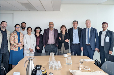
Publish Date: September 20, 2021
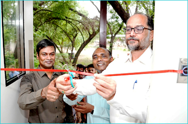
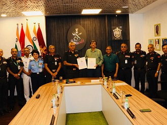
Advanced Electrical Characterization Facility Inaugurated at IIT Delhi
Share this on
Laboratory to enable measurement of electrical performance of devices and circuits used in electronic equipment
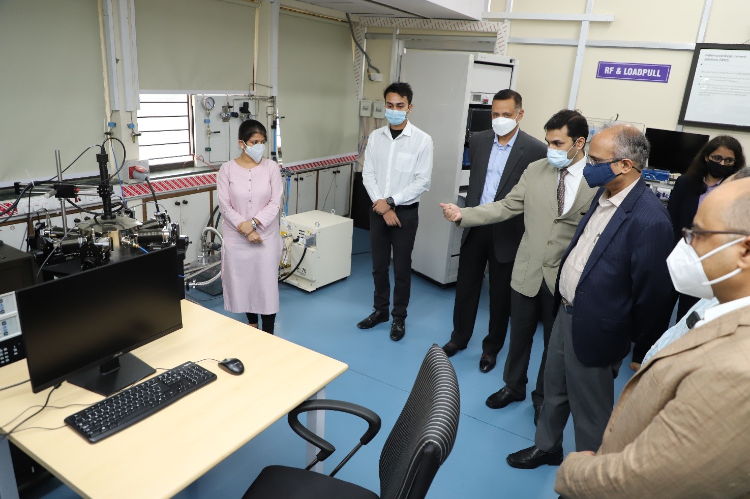
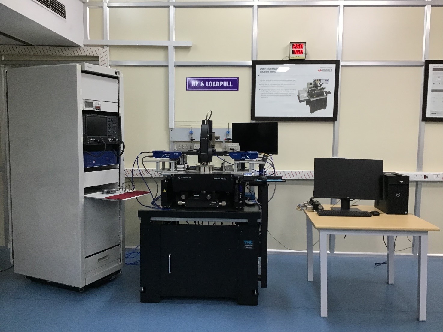
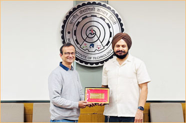
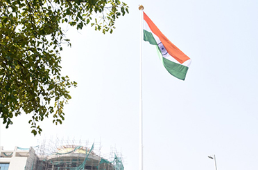
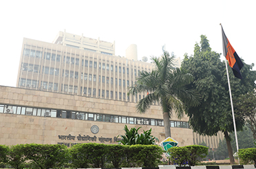
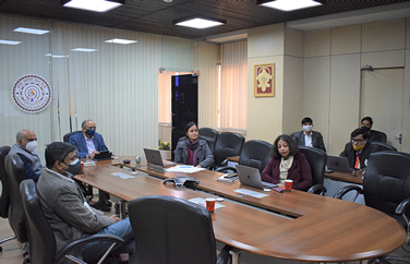
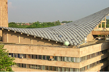
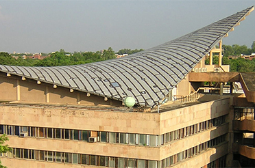
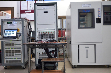
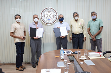
(Pic: Advanced Electrical Characterization Facility, IIT Delhi)
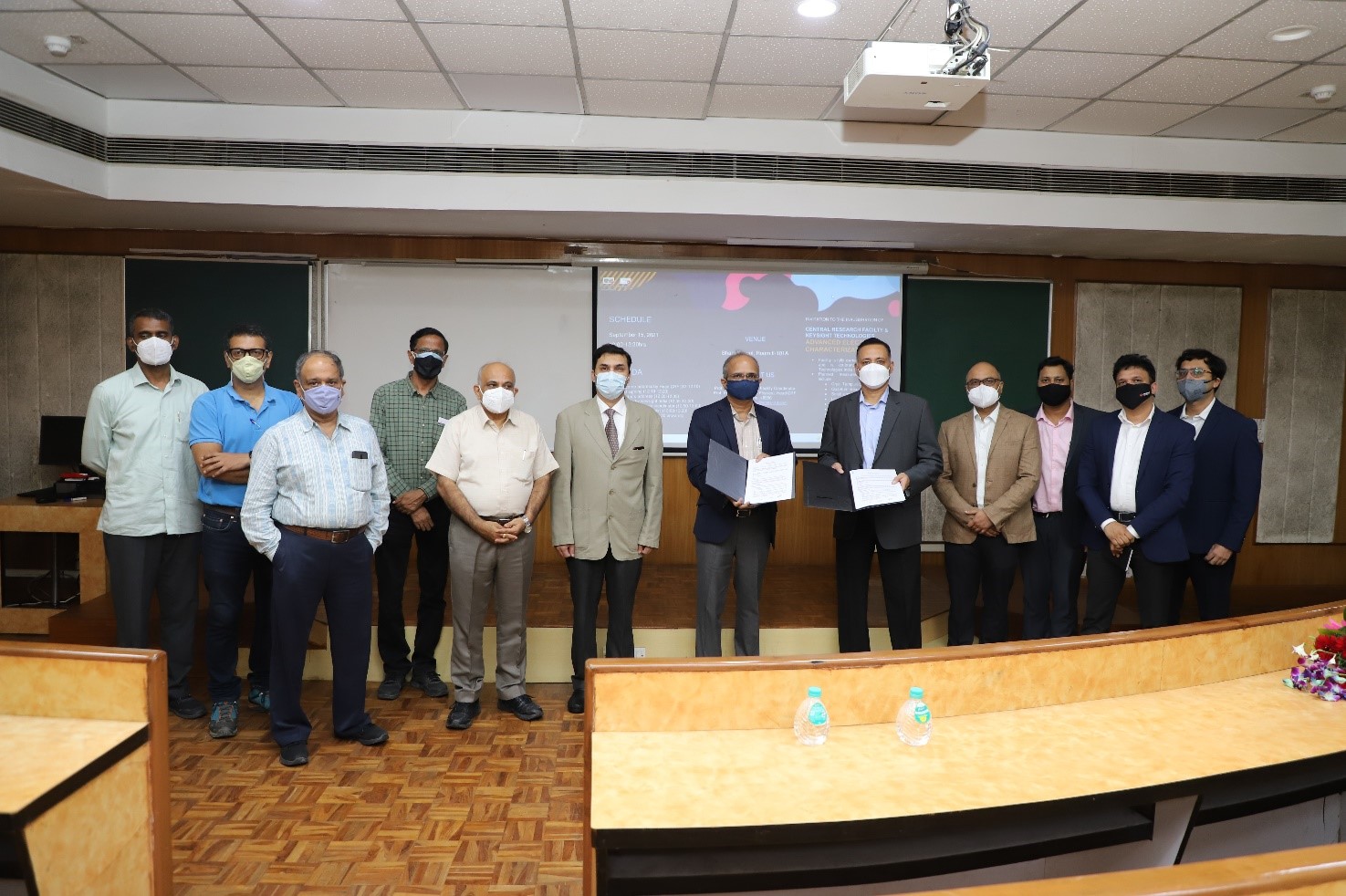
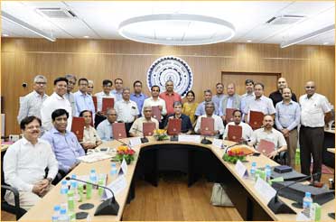
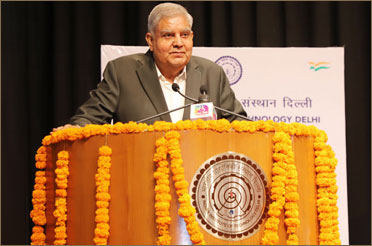
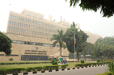
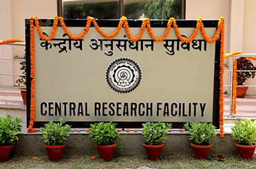
New Delhi: In another step towards further strengthening its position as one of the India’s finest research institutes in area of integrated electronic circuits and devices, IIT Delhi recently inaugurated Advanced Electrical Characterization Laboratory under the aegis of Central Research Facility.
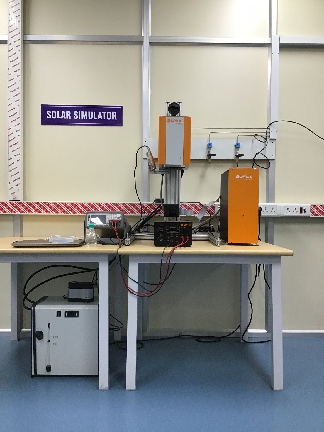
Setup with an invested cost of INR 17 Crores (equivalent of US$ 2.3M), this laboratory will enable measurement of electrical performance of devices and circuits that are used in electronic equipment, such as mobile phones, space satellites, and quantum computers to name a few. The facility will be accessible to various researchers of IIT Delhi as well as researchers from other institutions.
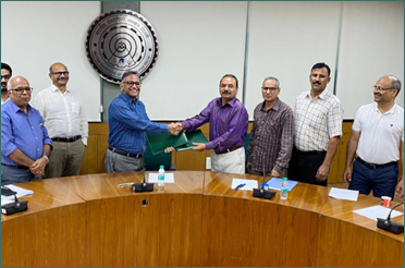
IIT Delhi has also signed an MoU with Keysight Technologies India Pvt Ltd. to co-brand the lab.
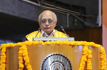
Speaking on the occasion, Prof. V. Ramgopal Rao, Director, IIT Delhi said, “IIT Delhi has significantly enhanced its research infrastructure in the last few years in the areas of Nano fabrication, materials characterization, testing and prototype manufacturing. This electrical characterization facility established with partial support from Keysight Technologies India Pvt Ltd is a welcome addition to the existing facilities in this area. IIT Delhi is also keen to collaborate with Keysight Technologies and other industries in this area to further strengthen its research activities in this space.”
Mr. Sudhir Tangri, Vice President and India Country General Manager at Keysight Technologies said, “This advanced electrical characterization facility enables researchers to perform complex electronic measurements with the highest level of precision to minimize uncertainties. It will accelerate research in semiconductors, DC-RF, and noise characterization. Keysight is excited to be part of the innovation journey.”
The laboratory in-charge, Prof. Abhisek Dixit from the Electrical Engineering Department, IIT Delhi said, “We are now equipped to perform various types of electrical measurements on a wide variety of packaged and on-wafer devices in a broad range of temperatures from 4.2K to +300 deg. C with the highest levels of precision possible anywhere in the world”.
**********
Other News
IIT Delhi Secures Top Three Awards at Sanrachna 2026: National Product Development & Design Hackathon for Technical Textiles
Read More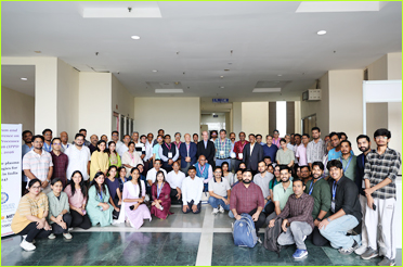
IIT Delhi Successfully Hosts IPPD 2026: International Conference Showcases Plasma Technologies for Sustainable Development under the "Plasma Pravah (प्रवाह): Legacy and Society Initiative"
Read More
आई.आई.टी. दिल्ली में "पर्यावरण एवं सततता" विषय पर सी.एस.आर. कॉन्क्लेव 2026; शोधकर्ताओं द्वारा विकसित प्रौद्योगिकी समाधानों का प्रदर्शन
Read More
IIT Delhi Organises CSR Conclave 2026 on Environment & Sustainability; Showcases Technology Solutions Developed by its Researchers
Read More
Online CEP certificate programme in "Certificate Programme in Applied Data Science & Artificial Intelligence: From Fundamentals to Deployment (Batch 04)".
Read More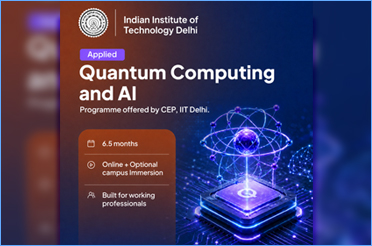
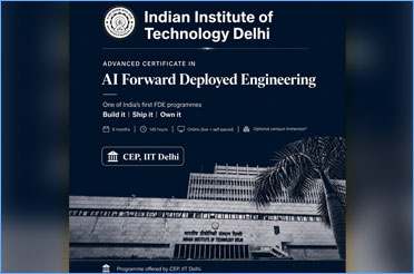
Online CEP certificate programme in "Advanced Certificate in AI Forward Deployed Engineering".
Read More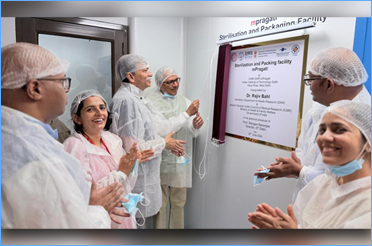
भारत के मेडटेक इकोसिस्टम को सुदृढ़ बनाने की दिशा में एक और कदम – आई.आई.टी. दिल्ली के mPragati में सी.एन.सी. तथा स्टेरिलाइज़ेशन व पैकेजिंग प्रयोगशाला का उद्घाटन
Read More
Strengthening India’s MedTech Ecosystem –CNC and Sterilization & Packaging Lab Inaugurated at mPragati, IIT Delhi
Read More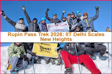

आई.आई.टी.–सोरबोन यूनिवर्सिटी की साझेदारी हुई और सशक्त: अनुसंधान, शिक्षा और नवाचार में फ्रांस-भारतीय साझेदारी का विस्तार
Read More
IIT Delhi and Sorbonne University Deepen Strategic Partnership, Expanding Franco-Indian Collaboration in Research, Education and Innovation
Read More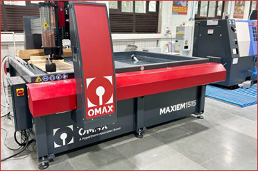
IIT Delhi and ICICI Foundation Inaugurate Advanced Smart Manufacturing and Bio-Innovation Facilities
Read More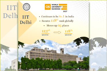
क्यू.एस. वर्ल्ड यूनिवर्सिटी रैंकिंग 2027: आई.आई.टी. दिल्ली ने अपनी वैश्विक रैंकिंग में दर्ज की उल्लेखनीय प्रगति, 118वाँ स्थान प्राप्त कर भारत में शीर्ष स्थान पर कायम
Read More
QS World University Rankings 2027: IIT Delhi Further Improves its Global Ranking, Achieves 118th Position; Continues to be No. 1 Indian Institute
Read More
आई.आई.टी. दिल्ली में युवा संगम चरण VI के अंतर्गत छत्तीसगढ़ के युवा प्रतिनिधिमंडल का स्वागत
Read More
भारत इनोवेट्स 2026: आई.आई.टी. दिल्ली ने रक्षा, कृत्रिम बुद्धिमत्ता (ए.आई.) और स्वास्थ्य सेवा के क्षेत्रों में नवाचारों का किया प्रदर्शन; वैश्विक अनुसंधान और नवाचार साझेदारियों को मिली मजबूती”
Read More

Bharat Innovates 2026: IIT Delhi Showcases Innovations Across Defence, AI, Healthcare; Strengthens Global Research and Innovation Partnerships
Read More
Selected candidate list for the PhD Program of the Department of Materials Science and Engineering for the session 2026-27, I Semester.
Read More
Online CEP certificate programme in "Executive Certificate programme on Textile Foundation"
Read More

आई.आई.टी. दिल्ली में केंद्रीय अनुसंधान सुविधा दिवस 2026 का आयोजन; उन्नत अनुसंधान अवसंरचना का प्रदर्शन
Read More
IIT Delhi Celebrates Central Research Facility (CRF) Day 2026, Showcases Advanced Research Infrastructure
Read More
आई.आई.टी. दिल्ली से युवा संगम चरण-VI के अंतर्गत 45-सदस्यीय दिल्ली युवा प्रतिनिधिमंडल छत्तीसगढ़ के लिए रवाना
Read More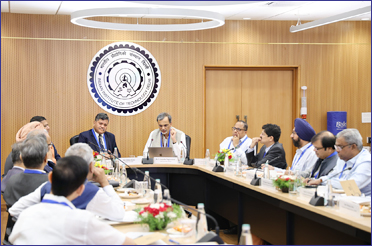
खाड़ी क्षेत्र में तनाव के बीच ऊर्जा सुरक्षा के विकल्पों पर विमर्श हेतु आई.आई.टी. दिल्ली में राष्ट्रीय संगोष्ठी का आयोजन
Read More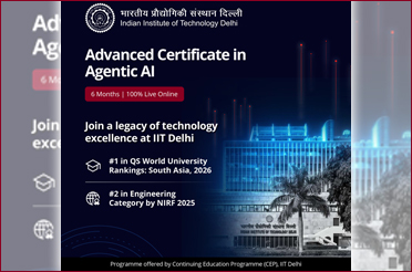
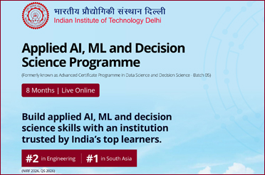
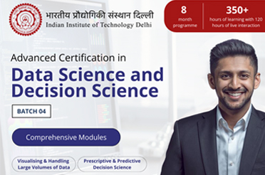
Online CEP certificate programme in "Applied AI, ML and Decision Science Programme (Formerly known as Advanced Certificate Programme in Data Science and Decision Science - Batch 06)"
Read More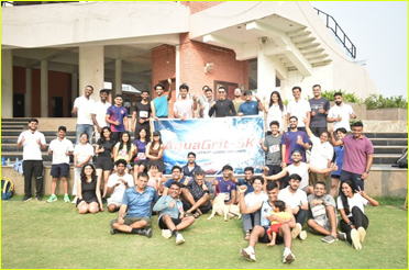
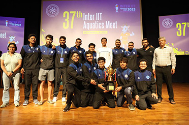
AquaGrit-5K 2026 Brings Together Endurance, Team Spirit and Campus Fitness Culture at IIT Delhi
Read More
IIT Delhi Flags Off 45-Member Delhi Youth Delegation to Chhattisgarh Under Yuva Sangam Phase VI
Read More
A National Seminar on Energy Security Held at IIT Delhi to Explore Options Amid Gulf Conflict
Read More
हाई स्कूल की छात्राओं हेतु भारतीय प्रौद्योगिकी संस्थान दिल्ली के STEM मेंटरशिप कार्यक्रम के पाँचवें बैच का ग्रीष्मकालीन चरण सफलतापूर्वक संपन्न।
Read More
IIT Delhi’s STEM Mentorship Program for High School Girls: Summer Phase of the 5th Batch Concludes Successfully
Read More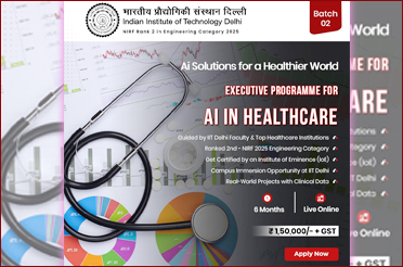
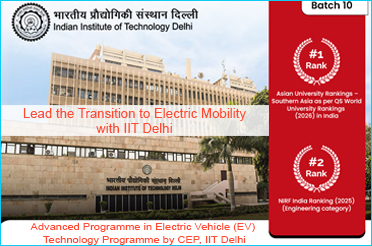
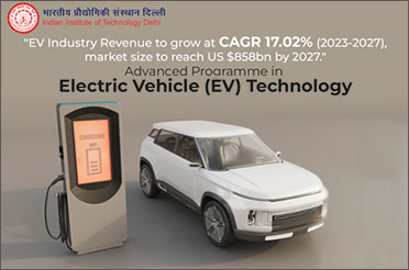
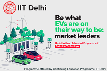
Online CEP certificate programme in "Advanced Programme in Electric Vehicle Technology ( Batch 10 )"
Read More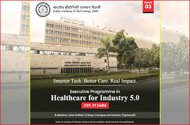
Online CEP certificate programme in "Executive Programme in Healthcare for Industry 5 .0 (Batch 3)"
Read More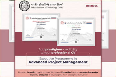
Online CEP certificate programme in "Executive Programme in Advanced Project Management ( Batch 05 )"
Read More


आई.आई.टी. दिल्ली संस्थान में ‘जय भीम सप्ताह 2026’ का आयोजन: डॉ. भीमराव अंबेडकर की विरासत को समर्पित चिंतन, संवाद और सहभागिता का एक सप्ताह
Read More
Online CEP certificate programme in "Idea To Product (ITP): Ideation, Innovation, Intellectual Property & Commercialization"
Read More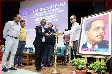
IIT Delhi Celebrates ‘Jai Bhim Saptaha 2026’: A Week of Reflection, Dialogue, and Participation Commemorating the Legacy of Dr. B.R. Ambedkar
Read More
ICEF Report: IIT Delhi Researchers Call for Examining Systemic and Socio-Economic Dimensions of India's Energy Transition
Read More
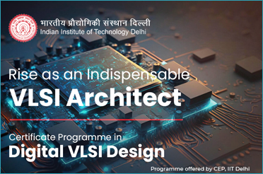
Online CEP certificate programme in "Certificate Programme in Digital VLSI Design (Batch 02)"
Read More
फ्लिपकार्ट के सह-संस्थापक और आई.आई.टी. दिल्ली के पूर्व विद्यार्थी बिन्नी बंसल द्वारा संस्थान में उनके नाम पर रखे गए एक प्रदर्शनी हॉल का उद्घाटन
Read More
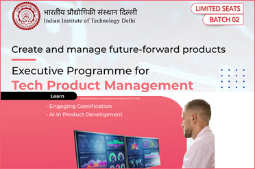
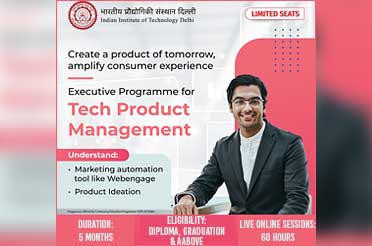
Online CEP certificate programme in "Executive Programme in Tech Product Management (Batch 04)"
Read More
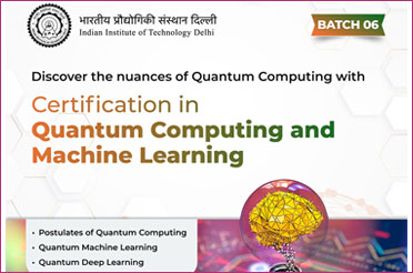
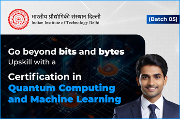
Online CEP certificate programme in "Certification in Quantum Computing and Machine Learning (Batch 08)"
Read More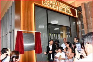
Flipkart Co-founder and IIT Delhi Alum Binny Bansal Inaugurates an Exhibition Hall Named After Him at the Institute
Read More
Online CEP certificate programme in "Executive Programme in Supply Chain and Operations Analytics - (Batch 03)"
Read More
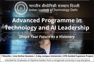
Online CEP certificate programme in "Advanced Programme in Technology and AI Leadership - Batch 03"
Read More
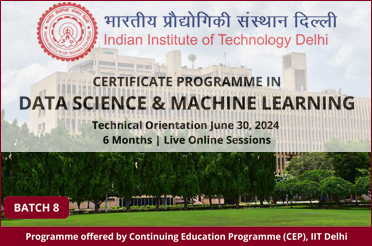
Online CEP certificate programme in "Certificate Programme in Data Science, AI and Machine Learning- Batch 12"
Read More
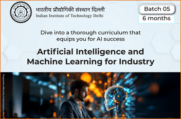
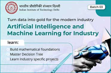
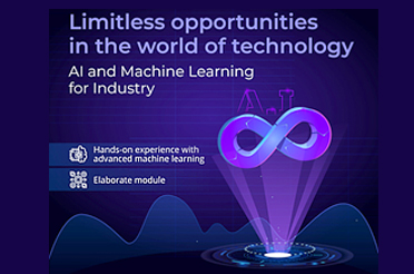
Online CEP certificate programme in "Artificial Intelligence and Machine Learning for Industry (Batch 8)"
Read More
क्यू.एस. विषय रैंकिंग 2026: आई.आई.टी. दिल्ली पांच प्रमुख विषयों में दुनिया के शीर्ष 50 में; भारत के शीर्षतम इंजीनियरी एवं प्रौद्योगिकी संस्थान के रूप में कायम
Read More
QS Subject Rankings 2026: IIT Delhi in Global Top 50 in Five Major Subjects, Continues as the No. 1 Engineering & Technology Institute in India
Read More
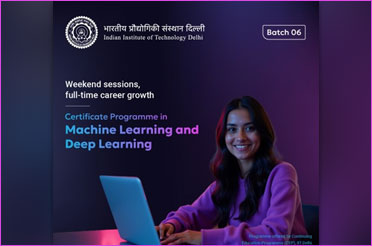
Online CEP certificate programme in "Advanced Certificate Programme in AI, ML and DL ( formerly known as Certificate Programme in Machine Learning and Deep Learning ) ( Batch 8)"
Read More
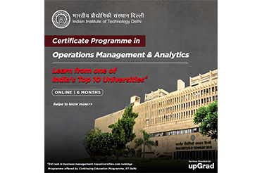
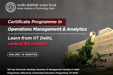
Online CEP certificate programme in "Executive Programme in Operations Management and Analytics (Batch 7)"
Read More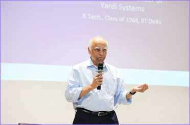
Alumnus Anant Yardi Pledges Transformational Gift to Strengthen AI Leadership and Campus Infrastructure at IIT Delhi | आई.आई.टी. दिल्ली में ए.आई. नेतृत्व और परिसर अवसंरचना के सुदृढ़ीकरण की दिशा में पूर्व विद्यार्थी अनंत यार्डी का दूरदर्शी योगदान।
Read More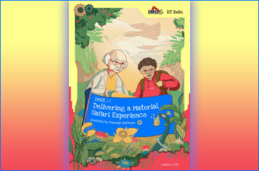
IIT Delhi’s DMSE Launches First-of-its-Kind Comic Book–Style Brochure to Demystify Complex Scientific Concepts | आई.आई.टी. दिल्ली के पदार्थ विज्ञान एवं इंजीनियरी विभाग ने अपनी तरह की पहली कॉमिक बुक शैली का ब्रोशर लॉन्च किया
Read More
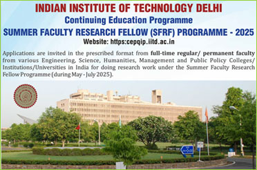
Summer Research Fellowship Programme 2026 at IIT Delhi (For Undergraduate & Postgraduate Students)
Read More
Mercedes-Benz Research and Development India and IIT Delhi Collaborate for Joint Research | मर्सिडीज‑बेंज रिसर्च एंड डेवलपमेंट इंडिया और आई.आई.टी. दिल्ली ने संयुक्त अनुसंधान के लिए साझेदारी की
Read More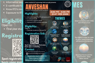
IIT Delhi to Organise Anveshan 2026 for Final-Year UG and PG Students on March 21 | आई.आई.टी. दिल्ली स्नातक (यू.जी.) और स्नातकोत्तर (पी.जी.) के अंतिम वर्ष के विद्यार्थियों के लिए 21 मार्च को “अन्वेषण 2026” का आयोजन करेगा
Read More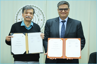
ISA and IIT Delhi Deepen Partnership to Advance Solar Skills Across Member Countries | आई.एस.ए. (ISA) और आई.आई.टी. दिल्ली ने सदस्य देशों में सौर कौशल को बढ़ावा देने की दिशा में की मजबूत साझेदारी
Read More
IIT Delhi Signs MoU with Jindal Steel to Establish Nodal Centre of Excellence for Structural Steel Research and Innovation | संरचनात्मक स्टील अनुसंधान में नया कदम: आई.आई.टी. दिल्ली ने जिंदल स्टील के साथ समझौता ज्ञापन पर किया हस्ताक्षर
Read More
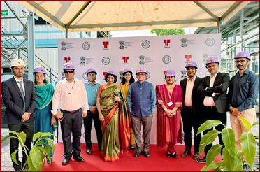
Union Minister for Education Shri Dharmendra Pradhan Lays Foundation Stones for Academic Block and Girls Hostel at IIT Delhi | केंद्रीय शिक्षा मंत्री श्री धर्मेंद्र प्रधान द्वारा आई.आई.टी. दिल्ली में शैक्षणिक खंड एवं महिला छात्रावास का शिलान्यास
Read More
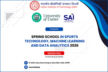
Online CEP workshop programme in "Spring School in Sports Technology, Machine Learning and Data Analytics 2026 ( under the initiative IIT Delhi–SAI–University of Exeter Sports Technology Workshop )"
Read More
अ.जा./अ.ज.जा. समुदाय के पीएच.डी. शोधार्थियों के लिए ‘STEMM में परिवर्तनकारी नेतृत्व’ कार्यशाला के तीसरे संस्करण का सफल आयोजन | Third Edition of Transformative Leadership in STEMM Workshop for Ph.D. Scholars from SC/ST Community Held
Read More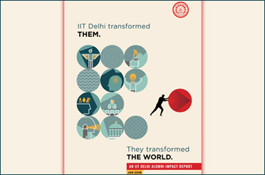
संस्थान के 68वें स्थापना दिवस के अवसर पर पहली ‘अल्युमनी इम्पैक्ट रिपोर्ट’ का विमोचन" | IIT Delhi Alumni Impact Report
Read More
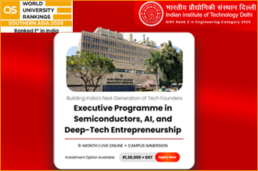
“सेमीकंडक्टर्स, ए.आई. और डीप टेक उद्यमिता में कार्यकारी ऑनलाइन CEP प्रमाणपत्र कार्यक्रम” | Online CEP certificate programme in "Executive Programme in Semiconductors, AI, and Deep-Tech Entrepreneurship"
Read More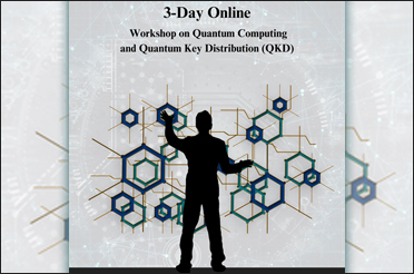
क्वांटम कंप्यूटिंग और क्वांटम की (Key) डिस्ट्रीब्यूशन (QKD) पर 3-दिवसीय ऑनलाइन कार्यशाला | Online CEP workshop programme in "3 - Day Online Workshop On Quantum Computing And Quantum Key Distribution (QKD)"
Read More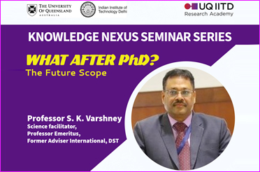
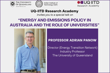
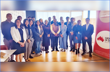
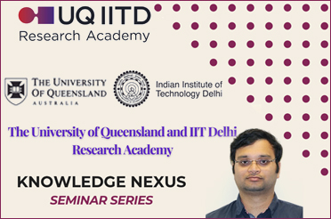
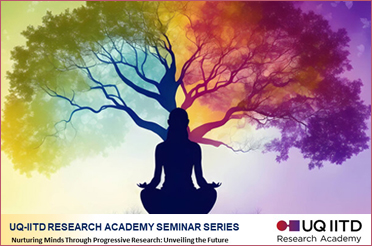
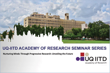
यू.क्यू. आई.आई.टी.डी. (UQ–IITD)- नॉलेज नेक्सस सेमिनार श्रृंखला | UQ IITD - KNOWLEDGE NEXUS SEMINAR SERIES
Read More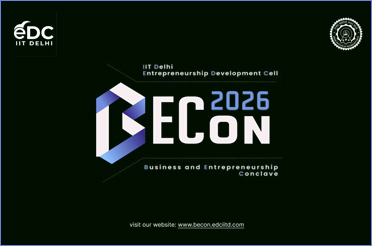
उद्यमिता विकास प्रकोष्ठ (eDC), आई.आई.टी. दिल्ली द्वारा BECon’26 का आयोजन | Entrepreneurship Development Cell (eDC), IIT Delhi to Organise BECon’26, One of India’s Largest Student-Led Entrepreneurship Summits
Read More
आई.आई.टी. दिल्ली में गणतंत्र दिवस 2026 की झलकियाँ | In Pics- Republic Day 2026 Celebrations at IIT Delhi
Read More
आई.आई.टी. दिल्ली ने मनाया अपना 68वां स्थापना दिवस: 'अल्युमनी इम्पैक्ट रिपोर्ट' की गई जारी | IIT Delhi Celebrates its 68th Foundation Day, Releases Alumni Impact Report
Read More

आई.आई.टी. दिल्ली के #एक्सपीरियंसआईआईटीडी के तहत जे.ई.ई. 2026 के अभ्यर्थियों के लिए कोटा, राजस्थान में ओपन हाउस का आयोजन | IIT Delhi to Organise Open House for JEE 2026 Aspirants in Kota, Rajasthan, Under its Flagship Outreach Initiative #ExperienceIITD
Read More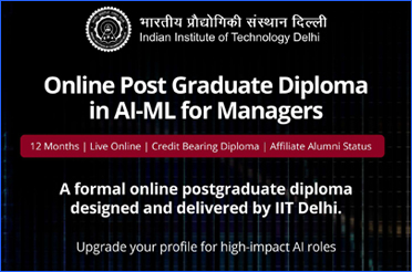
प्रबंधकों के लिए कृत्रिम बुद्धिमत्ता-मशीन लर्निंग में ऑनलाइन स्नातकोत्तर डिप्लोमा | Online CEP certificate programme in "Online Post Graduate Diploma in AI-ML for Managers"
Read More
आई.आई.टी. दिल्ली ने युवा संकायों को शोध में सशक्त बनाने के लिए की दीपक राघवन फैमिली फाउंडेशन एक्सेलरेटर कार्यक्रम की शुरुआत | IIT Delhi Launches Deepak Raghavan Family Foundation Accelerator Program to Strengthen Young Faculty in Research
Read More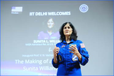
आई.आई.टी. दिल्ली में नासा एस्ट्रोनॉट सुनीता विलियम्स का व्याख्यान: ‘द मेकिंग ऑफ एन एस्ट्रोनॉट: सुनीता विलियम्स स्टोरी' | NASA Astronaut Sunita Williams Delivers a Talk at IIT Delhi: 'The Making of an Astronaut: Sunita Williams' Story’
Read More
आई.आई.टी. दिल्ली ने समावेशिता को दिया बढ़ावा, इंटर-कॉलेज समावेशी खेल समारोह 'SANGAM 2026' का सफल समापन | IIT Delhi Champions Inclusion as Inter-College Inclusive Sports Meet ‘SANGAM 2026’ Concludes Successfully
Read More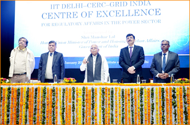
आई.आई.टी. दिल्ली में विद्युत क्षेत्र में विनियामक मामलों के लिए उत्कृष्टता केंद्र का शुभारंभ | Centre of Excellence for Regulatory Affairs in the Power Sector Launched at IIT Delhi
Read More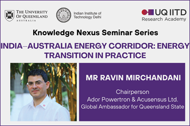
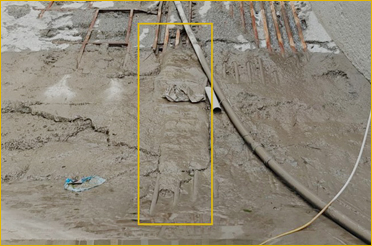
हाइड्रोलिक संरचनाओं की मरम्मत में अल्ट्रा-हाई-परफॉर्मेंस फाइबर-रीइन्फोर्स्ड कंक्रीट का अनुप्रयोग | Application of Ultra-High-Performance Fiber-Reinforced Concrete for Repair of Hydraulic Structures
Read More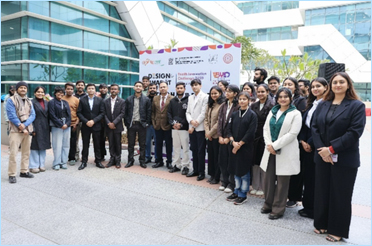
डिज़ाइन फ़ॉर भारत – यूथ इनोवेशन चैलेंज 2026’ के अंतर्गत आई.आई.टी. दिल्ली में एक डिज़ाइन प्रदर्शनी का आयोजन | A Design Exhibition Under Design for Bharat—Youth Innovation Challenge 2026 Held at IIT Delhi
Read More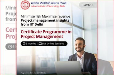
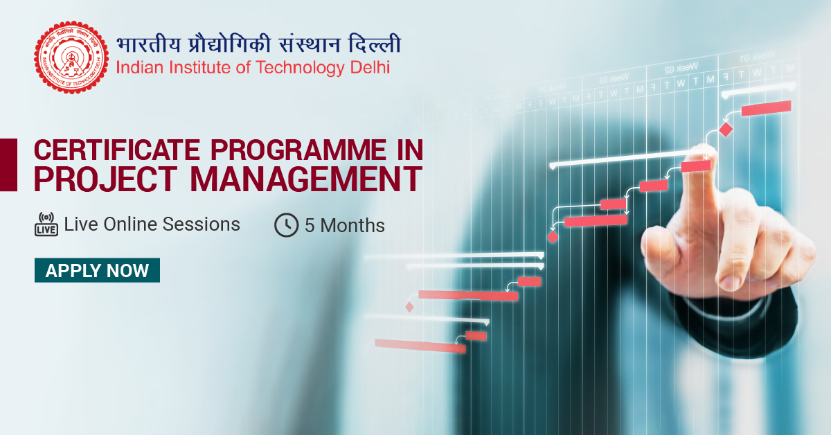
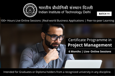
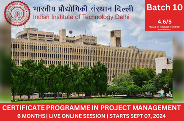
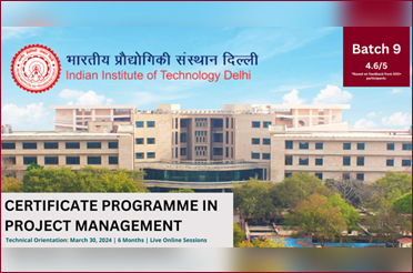
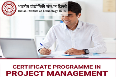
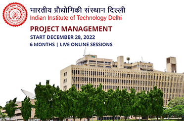
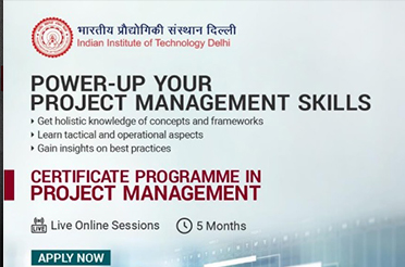
परियोजना प्रबंधन में सर्टिफिकेट प्रोग्राम (बैच–15) | Online CEP certificate programme in "Certificate Programme in Project Management ( Batch-15 )"
Read More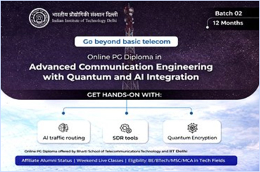
एडवांस्ड कम्युनिकेशन इंजीनियरिंग विद क्वांटम एंड एआई इंटीग्रेशन में ऑनलाइन पीजी डिप्लोमा (बैच-2) | Online PG Diploma in Advanced Communication Engineering with Quantum and AI Integration (Batch-2)
Read More
आई.आई.टी. दिल्ली के शैक्षणिक सत्र 2000 के विद्यार्थियों द्वारा संस्थान को रु. 70 करोड़ से अधिक के दान की घोषणा | IIT Delhi’s Batch of 2000 Commits Record ₹70+ Crore Pledge at Silver Jubilee Reunion
Read More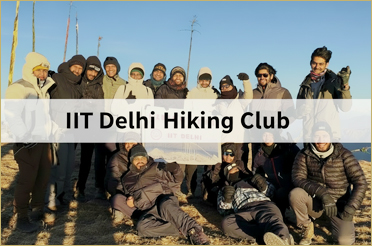
ठंडे हाथ और दिलों में गर्माहट: आई.आई.टी. दिल्ली हाइकिंग क्लब की शीतकालीन ट्रेक्स 2025 | Cold Hands and Warm Hearts: IIT Delhi Hiking Club’s Winter 2025 Treks
Read More
IIT Delhi Announces to Name its Exhibition Hall in Honor of Alumnus Binny Bansal, Celebrating Transformative Alumni Giving
Read More
Online CEP certificate programme in "Applied Data Science & Artificial Intelligence: From Fundamentals to Deployment - Batch 03"
Read More
Online CEP certificate programme in "Advanced Programme in Electric Vehicle Technology-Batch 09"
Read More
Online CEP certificate programme in "Online PG Diploma in Healthcare Product Development and Management (Batch-2)"
Read More
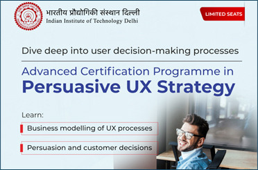
Online CEP certificate programme in "Advanced Certificate in AI-led UX and CX innovation for leadership (Formerly known as, “Advanced Certification Programme in Persuasive UX Strategy”) Batch 3"
Read More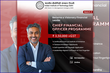
4th Edition of “Manasvi: a STEM Mentorship Program for High School Girls” by IIT Delhi Concludes Successfully
Read More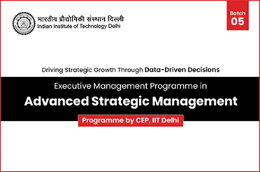
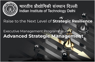
Online CEP certificate programme in "Executive Management Programme in Advanced Strategic Management (Batch 05)."
Read More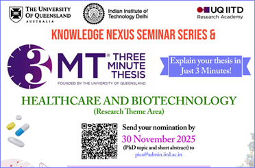
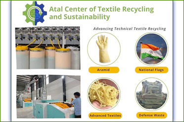
Centre Set Up Under IIT Delhi Transfers Technologies for Recycling of Technical Textiles, Defence Grade Fibers, and the National Flag
Read More
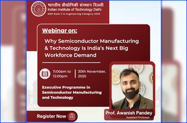
Executive Programme in Semiconductor Manufacturing and Technology offered through CEP, IIT Delhi.
Read More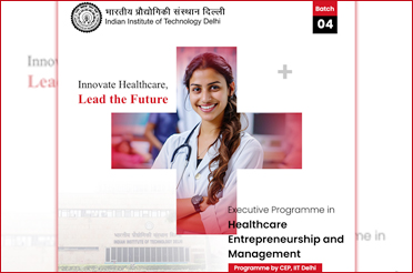
Online CEP certificate programme in "Executive Programme in Healthcare Entrepreneurship and Management (Batch 04)"
Read More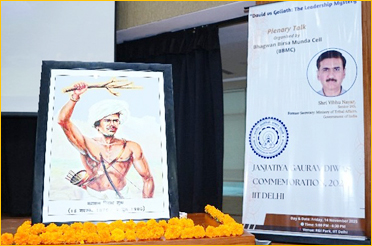
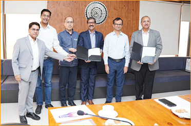
IIT Delhi Partners with Yamaha Motor Solutions India to Drive Impactful Research in Emerging Technologies
Read More


IIT Delhi and ERLDC Collaborate to Develop AI-Enabled Smart Device for Demand Side Energy Management
Read More
IIT Delhi’s First-Year B.Tech. Students Showcase Their Skills to Tackle Real-World Problems
Read More
Online CEP certificate programme in "Artificial Intelligence and Machine Learning for Industry-Batch 07"
Read More
Unnat Bharat Abhiyan Completes 11 Successful Years of Transforming Rural India Through Higher Education Institutions
Read More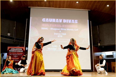
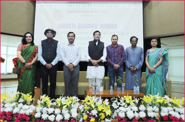
IIT Delhi Celebrates Janjatiya Gaurav Divas with a Vibrant Cultural Evening Honouring India’s Tribal Heritage
Read More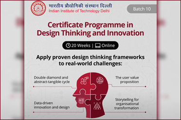
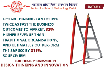
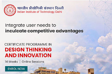
Online CEP programme in "Certificate Programme in Design Thinking and Innovation-Batch 10"
Read More
IIT Delhi Organises Open House; Showcases Cutting-Edge Research and Innovative Projects to Students, Industry, and Funding Agencies
Read More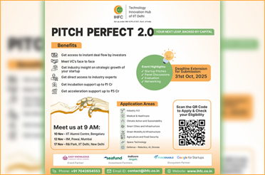
IIT Delhi’s Technology Innovation Hub IHFC to Launch ‘Pitch Perfect 2.0’ — a Flagship Pitching Initiative for Startups
Read More
IIT Delhi Celebrates Janjatiya Gaurav Divas with Thoughtful Tributes and Inspiring Dialogues
Read More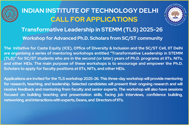
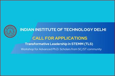
CALL FOR APPLICATIONS: Transformative Leadership in STEMM (TLS) 2025-26. Workshop for Advanced Ph.D. Scholars from SC/ST community
Read More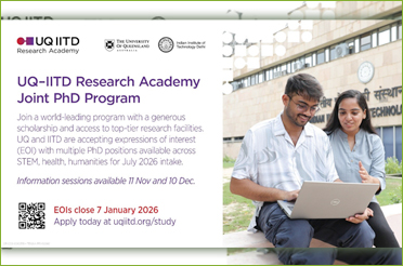
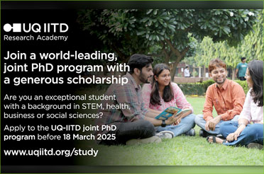
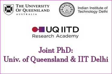
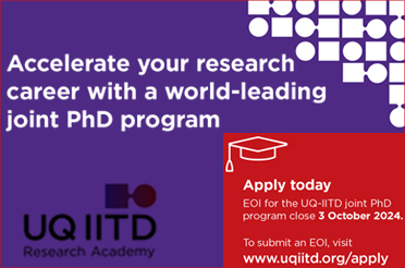
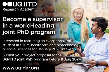
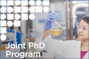
University of Queensland and IIT Delhi Open Applications for Joint PhD Programme Commencing July 2026
Read More
KVS and IIT Delhi Sign an MoU to Collaborate on Strengthening STEM Education in Schools for Students and Teachers
Read More
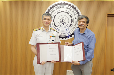
Indian Navy’s Directorate of Naval Architecture Signs MoU with IIT Delhi for Crew Centred Aspects of Warship Design
Read More
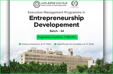
Online CEP programme in "Executive Management Programme in Entrepreneurship Development ( Batch 4)"
Read More
IIT Delhi and Samco Inc., Japan, Join Hands to Boost Semiconductor and High-Efficiency Silicon Solar Cell Research
Read More
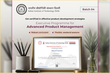
Online CEP programme in "Executive Programme for Advanced Product Management ( Batch 04 )"
Read More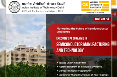
Online CEP programme in "Executive Programme in Semiconductor Manufacturing and Technology (Batch 2)"
Read More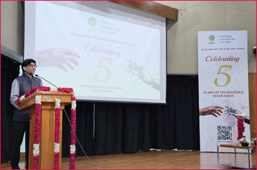
IHFC, the TIH of IIT Delhi, Showcases 25 Cutting-Edge Technologies to Mark its 5th Anniversary
Read More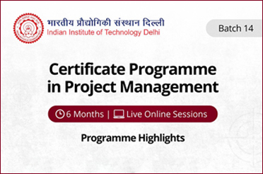
Adi Karmayogi Student Chapters Launched at IITs, IIMs, AIIMS, NITs and Top Institutions – Empowering Tribal Youth as Leaders, Innovators, and Change-Makers
Read More
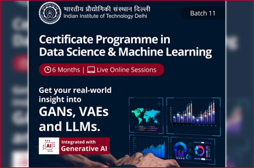
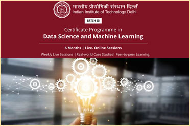
Online CEP programme in "Certificate Programme in Data Science and Machine Learning ( Batch - 11)"
Read More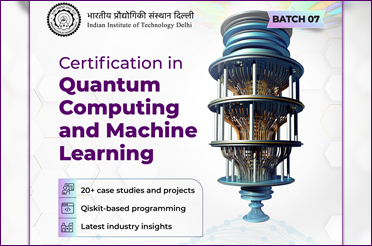
Online CEP programme in "Certification in Quantum Computing and Machine Learning (Batch 07)"
Read More
Shri Dharmendra Pradhan, Minister of Education, Inaugurates Key Programs and Startup Incubator at IIT Delhi - Abu Dhabi, Reinforcing a Landmark Bilateral Partnership
Read More
SAI NCSSR and IIT Delhi Sign MoU to Give Impetus to Wider Use of Sports Science and Innovation in India
Read More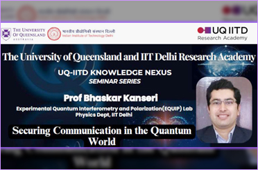
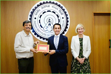
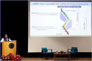
CEO of ANRF Delivers an Insightful Institute Lecture titled “ANRF Vision: Catalyzing India’s Rise as a Research and Innovation Powerhouse” at IIT Delhi
Read More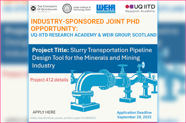
IIT Delhi Inaugurates Biosafety Level 3 Research Facility to Foster Research Involving Highly Infectious Pathogens
Read More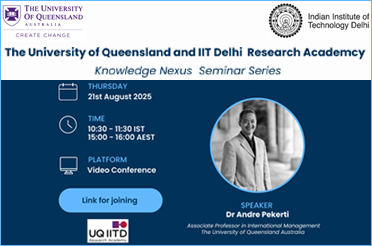

IIT Delhi and Wadhwani Foundation Inaugurate Centre of Excellence in Precision & Personalized Healthcare under Wadhwani Innovation Network
Read More


Union Minister of Textiles Launches Report on Handloom Carbon Footprint Assessment Prepared by IIT Delhi and DC (Handlooms)
Read More
Online CEP programme in "Certificate Programme for Future Tech Leaders AI & Industry 5.0 (Batch 1)"
Read More
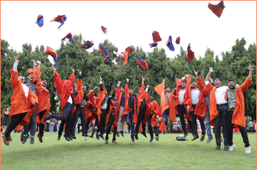
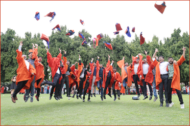
56th Convocation: 2764 IIT Delhi Students Awarded Degrees and Diplomas; Chief Guest Dr. Tessy Thomas, the Missile Woman of India, Inspires Graduating Students
Read More
IIT Delhi to Hold 56th Convocation on August 2, 2025; the Missile Woman of India, Dr. Tessy Thomas, to be the Chief Guest
Read More
Online PG Diploma programme in "Online PG Diploma In Healthcare Product Development And Management".
Read More
Online PG Diploma programme in "Online PG Diploma In Advanced Communication Engineering With Quantum And AI Integration".
Read More
Online CEP programme in "Executive Programme In Generative AI And Next Gen Digital Engineering (Batch 1 )".
Read More
Online CEP programme in "Executive Programme In Augmented Reality & Virtual Reality (Batch - 2 )".
Read More


Workshop on ‘Future Ready Energy Education: Opportunities and Challenges’ Held at IIT Delhi
Read More


Change Makers 2025 Summer Bootcamp Successfully Culminates at IIT Delhi with High School and 1st Year UG Students Presenting Promising Innovative Solutions to Environmental Challenges
Read More


QS World University Rankings 2026: IIT Delhi Features in List of Top 125 World Institutions; Emerges as No. 1 Educational Institute in India
Read More
IIT Delhi and LG Electronics Partner to Drive Innovation in Sustainable Home Appliance Technologies
Read More

World Environment Day 2025 Celebrated at IIT Delhi; Institute Highlights Need for Collective Action
Read More

IIT Delhi to Organise Open House in Delhi, Mumbai and Bengaluru for JEE Advanced 2025 Qualified Candidates
Read More
IIT Delhi launches new undergraduate programme BS in Chemistry for JEE (Advanced) 2025 qualified candidates
Read More

Central Electricity Regulatory Commission, IIT Delhi and Grid Controller of India sign MoU to Establish Centre of Excellence for Regulatory Affairs in Power Sector
Read More

Provisional Waiting List of Candidates for the Ph.D. Program in Materials Science and Engineering
Read More

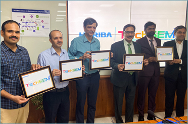
HORIBA India Join Hands with IIT Delhi to Support Three Technical Development Research Projects
Read More
Provisional *List of Selected Candidates for Ph.D. in Materials Science and Engineering, *Subject to Document Verification by the Academic Section DMSE
Read More


IIT Delhi Hosts ‘Manasvi: STEM Mentorship Program for High School Girls’ – Empowering Young Girls with Exposure and Opportunities to Become Future-Ready for STEM
Read More
IIT Delhi Debuts Online Post Graduate Diplomas to Empower Next-Gen Technological Leadership
Read More
Manufacturing Innovation Show: Agricultural Machineries, On-road Power Generation Device Among Several Prototypes Developed by 1st Year IIT Delhi UG Students
Read More


IIT Delhi Establishes a Chair on Applied AI for Sustainable Systems in Collaboration with R Systems
Read More
Fuelling a Sustainable Future: IIT Delhi-Abu Dhabi Announces Second Intake for Post-Graduate Energy & Sustainability Programs
Read More

IIT Delhi Successfully Conducts CAIC Student Elections Through E-Voting, Eyes Scaling to Larger Platforms
Read More

Shortlisted candidates list & shortlisting Criteria for PhD admission in Textile department
Read More
Shortlisted candidates list & shortlisting Criteria for MTech admission in Textile department
Read More

IIT Delhi, Central Water Commission Sign MoU for Water Resources Management Through Data Science, AI and Machine Learning
Read More
IIT Delhi Celebrates the Legacy of Dr. B.R. Ambedkar with “Jai Bhim Saptah” – A Week of Reflection, Dialogue, and Action
Read More


Placement 2024-25: UG Students at IIT Delhi Secure 850 Unique Offers to Date, Highest in Last Three Years
Read More
Bhagwan Birsa Munda Cell at IIT Delhi Hosts Tribal Students and Youth for an Exposure Visit
Read More
Empowering the Future: Through NURTURE Program IHFC (TIH of IIT Delhi) Trains Over 50,000 SC/ST Students in Cutting-Edge Technologies
Read More
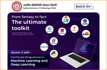
Online CEP programme in "Certificate Programme in Machine Learning and Deep Learning (Batch 6)."
Read More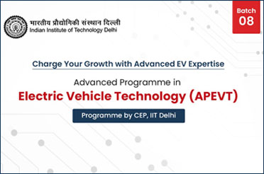
Online CEP programme in "Advance Programme in Electric Vehicle (EV) Technology (Batch 8)."
Read More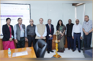
Quantum Materials & Devices (QMD) Hub at IIT Delhi Successfully Hosts its Grand Inception & Strategy Summit
Read More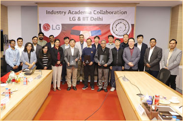
Online CEP programme in "Certificate Programme in Data Science & Machine Learning(Batch 10)"
Read More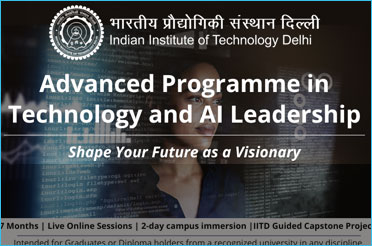
Online CEP programme in "Artificial Intelligence and Machine Learning for Industry (Batch 05)"
Read More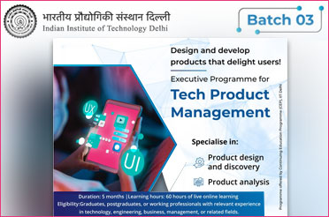

IIT Delhi Invites Applications from High Schoolers and 1st Year UG Students for Change Makers 2025 Summer Bootcamp
Read More
JAM Admission Portal JOAPS for Various Master’s Programs in IITs to Open from March 26, 2025
Read More
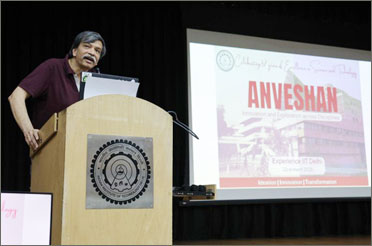
IIT Delhi organises ‘Anveshan 2025’ as a part of the Institute’s initiative of “Experience IITD”
Read More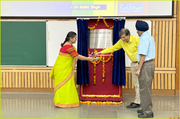
International Happiness Day Celebration marks the inauguration of Rekhi Mind Lab at IIT Delhi to promote Happiness Studies
Read More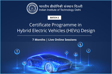
Online CEP programme in "Certificate Programme in Hybrid Electric Vehicles (HEVs) Design (Batch 2) "
Read More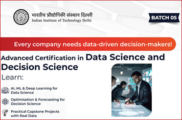
Online CEP programme in "Advanced Certification in Data Science and Decision Science (Batch 5) "
Read More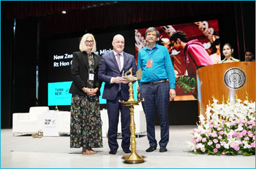
New Zealand Prime Minister Strengthens Academic Ties with India, Announces Scholarships at IIT Delhi
Read More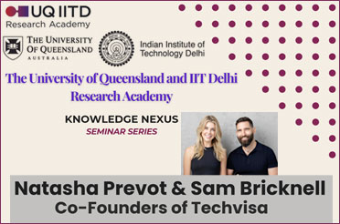
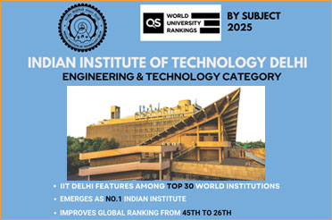
QS World University Rankings by Subject 2025: IIT Delhi Features Among Top 30 World Institutions in Engineering & Technology Category
Read More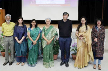
IIT Delhi to Organise an Insightful Event, “Anveshan: Innovation and Exploration Across Disciplines”, for Undergraduate and Postgraduate Students, Showcasing Curriculum, Research, and Campus Life
Read More
SANGAM, An Inclusive Intercollege Sports Event for Students with Disabilities, Held at IIT Delhi
Read More
Inaugural Chidambaram Memorial Lecture held at IIT Delhi on National Science Day; Prof Abhay Karandikar, DST Secretary, Delivered the Inaugural Lecture
Read More

Bhagwan Birsa Munda Cell at IIT Delhi Hosts an Exposure Visit for 200 Tribal Students from Five States
Read More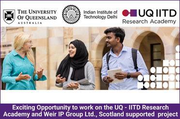
Opportunity to work on the UQ - IITD Research Academy and Weir IP Group Ltd., Scotland supported project
Read More
IIT Delhi Opens Its Doors to Teachers from Technical Institutions in Haryana for Skill Enhancement and Research-Driven Learning
Read More
IIT Delhi, IndiGo Sign MoU to Drive Innovation and Create Impactful Solutions for Airline Industry
Read More
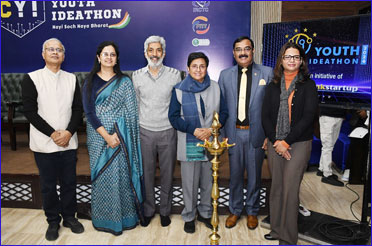
College Youth Ideathon 2025: An initiative to Fuel Innovation and Entrepreneurship Among India’s Youth Launched by IIT Delhi, MEPSC, and ThinkStartup
Read More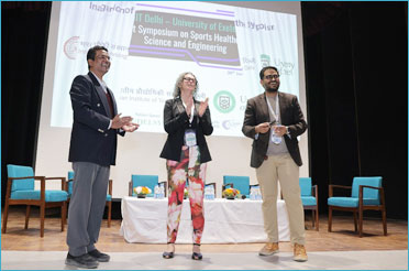
IIT Delhi and University of Exeter, UK, Host Joint Symposium on Sports Healthcare Science and Engineering
Read More
2nd Transformative Leadership in STEMM (TLS) Workshop for Ph.D. Scholars from SC/ST Community Held at IIT Delhi
Read More

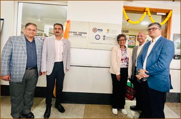
IHFC Collaborates with 10 Leading Institutions Across India to Launch Transformative Co-Innovation Centres (CiC) in Deep Tech, AI and Robotics
Read More
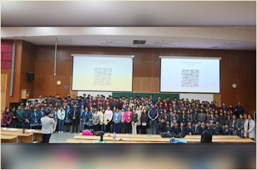
150 High School Students Attend Inaugural Lecture Under “Sci-Tech Spins” Lecture Series 2025 at IIT Delhi
Read More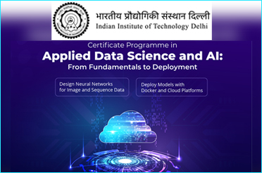
Online CEP programme "Certificate Programme in Applied Data Science & Artificial Intelligence: From Fundamentals to Deployment"
Read More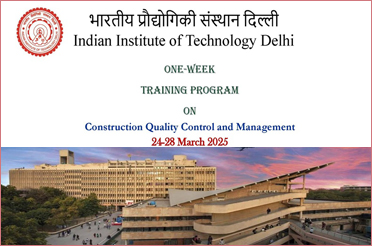
CEP programme "One-week Training Programme on Construction Quality Control and Management"
Read More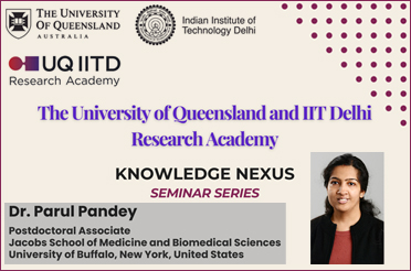
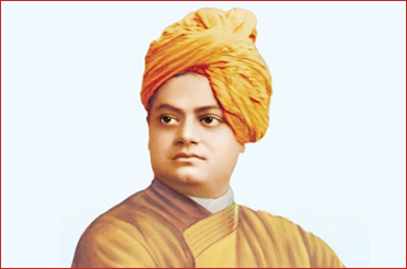
Swami Vivekananda Jayanti at IIT Delhi: Experts talk on Vedanta, Leadership, and India's Educational Legacy
Read More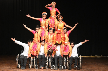
NISHAAN 2025, a Cultural Event Celebrating Diversity and Talent of Students with Disabilities, Organised at IIT Delhi
Read More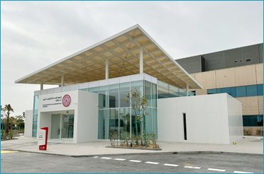
Third Batch of IIT Delhi’s STEM Mentorship Program for High School Girls Successfully Concludes
Read More
IIT Delhi Hosts Mr. Amandeep Singh Gill, UN Under-Secretary-General for Digital and Emerging Technologies and Secretary-General's Envoy on Technology, For a Discussion on AI Governance
Read More
Jake Sullivan, USA’s National Security Advisor, Delivers a Talk on 'The United States and India: Building a Shared Future' at IIT Delhi
Read More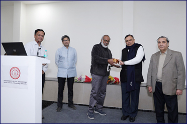
TRIP Centre, IIT Delhi, organizes a roundtable discussion on “Gendered Resilience in Transport: Enhancing Adaptation to Extreme Heat in Delhi”
Read More
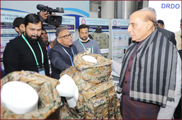
DRDO Industry Academia-Center of Excellence (DIA-CoE) at IIT Delhi Transfers Technology of ABHED, a Light Weight Bulletproof Jacket, to three Indian Industries
Read More
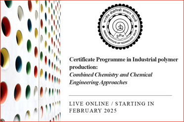
CEP programme on "Certificate Programme in Industrial Polymer Production: Combined Chemistry and Chemical Engineering Approaches"
Read More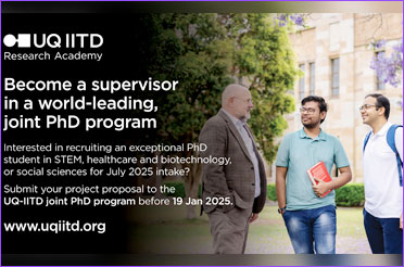

IIT Delhi Students Are Choosing Diverse Career Paths, Shows the Graduation Exit Survey 2024
Read More
DFPD Launches ‘Anna Chakra’ PDS Supply Chain Optimization Tool Developed by PSL, IIT Delhi
Read More

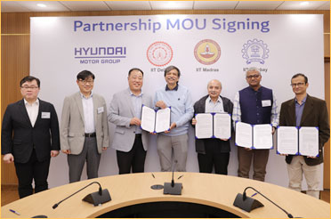
IIT Delhi Leads Landmark Collaboration with Hyundai Motor Group to Advance Battery and Electrification Research
Read More
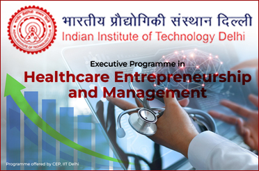
3rd online CEP programme on "Executive Programme in Healthcare Entrepreneurship and Management"
Read More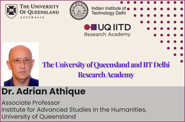
Bhagwan Birsa Munda Cell at IIT Delhi Hosts Commemoratives Events on Janjatiya Gaurav Diwas
Read More
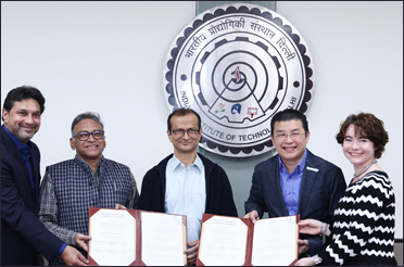
AIIMS New Delhi, IIT Delhi and UCL Announce Trilateral Partnership to Scale Up MedTech Innovation
Read More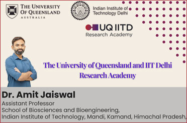

_1731498114.jpg)


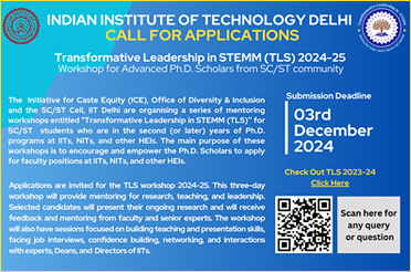
Call for Applications: Transformative Leadership in STEMM (TLS) Workshop for Advanced PhD Scholars from SC/ST community.
Read More
IIT Delhi and Centre for Railway Information Systems Partner to Transform Indian Railways Through Cutting-Edge Research
Read More
AI to Empower, Not Threaten: Meta's Chief AI Scientist Yann LeCun Calls for New Model Architectures at IIT Delhi
Read More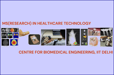
IIT Delhi Launches MS (Research) Program in ‘Healthcare Technology’ for Medical and Allied Clinical Professionals
Read More


Workshops Organised for Parents and School Kids to Raise Awareness and Co-Create Possible Solutions to Beat the Heat
Read More

Joint Report by IIT Delhi and IEA: "Clean Energy Innovation Policies in Emerging and Developing Economies"
Read More

PGDEx-VLFM Batch 07 Students Meet IIT Delhi Director; Witness an Inspiring Interactive Session
Read More
IIT Delhi, IAF Join Hands for AI-powered Research on Technical Textiles; to Focus on Parachute and Other Safety Equipment
Read More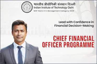
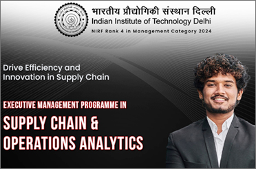
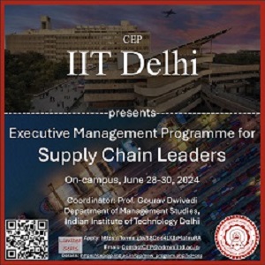
4th online CEP programme "Executive Management Programme in Supply Chain & Operations Analytics"
Read More
India's first-of-its-kind DST Supported CO2-to-Methanol Pilot Plant Project to be Implemented by IIT Delhi and Thermax Ltd. in PPP Mode
Read More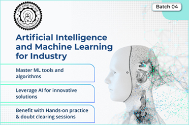
Major Milestones for IIT Delhi as His Highness Sheikh Khaled bin Mohamed Visits Abu Dhabi Campus
Read More
IIT Delhi and Systra Group Sign MoU to Collaborate on Research Advancing Sustainable Development Goals
Read More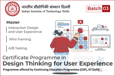
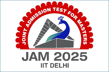
Joint Admission Test for Masters (JAM) 2025: Application window opens on 3rd September 2024
Read More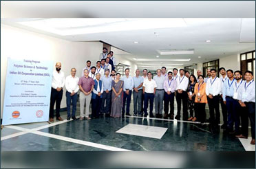
Materials Science and Engineering Dept. at IIT Delhi Hosts Training Program on ‘Polymer Science and Technology’ for IOCL Executives
Read More
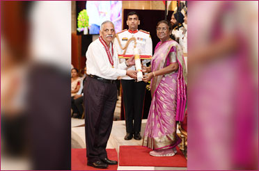
Rashtriya Vigyan Puraskar 2024: Prof. Bhim Singh, SERB National Science Chair and Emeritus Professor at IIT Delhi, Honored with the Vigyan Shri Award
Read More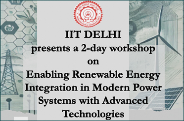
CEP programme "Workshop on Enabling Renewable Energy Integration in Modern Power Systems with Advanced Technologies"
Read More
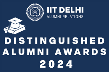
IIT Delhi Honors Alumni with Prestigious Distinguished Alumni Awards 2024 at 55th Convocation Ceremony
Read More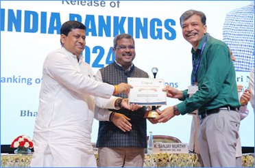
IIT Delhi to Hold its 55th Convocation on August 10, 2024; Shri. Hari S. Bhartia, Founder and Co-Chairman, Jubilant Bhartia Group to be Chief Guest
Read More
Important Information for PhD students regarding seating of Guests in Dogra Hall in 1st Phase
Read More
IIT Delhi Develops Two Pioneering Healthcare Technologies; Successfully Transfers them to Industry
Read More
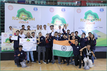
DD Robocon India 2024: Nirma University from Gujarat Wins Robotics Competition; Maharashtra’s Pimpri Chinchwad College of Engineering Secures Runner-up Position
Read More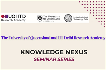
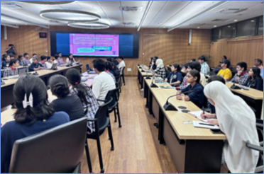
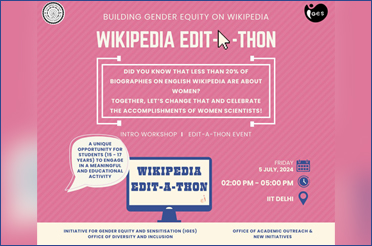
Initiative for Gender Equity and Sensitisation (IGES) at IIT Delhi to Organise Wikipedia Edit-a-Thon on July 5
Read More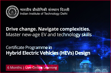
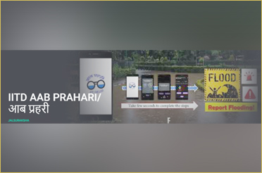
Bridging the Gap: IIT Delhi’s Aab Prahari App Enables Citizens to Report Real-Time Flooding Incidents and Help Civic Agencies During Monsoon
Read More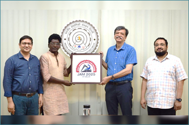
An Open House for All JEE (Advanced) 2024-Qualified Candidates Aspiring to Join IIT Delhi’s Hauz Khas Campus in India or Abu Dhabi Campus in UAE to be Organised on June 15, 2024
Read More

Students Clearing JEE Advanced 2024 can apply for Admissions to IIT Delhi-Abu Dhabi Campus
Read More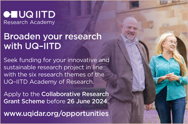
UQ-IITD Research Academy - Promotion of the Call for Collaborative Research grant applications
Read More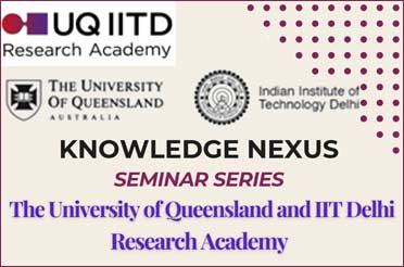
Entrepreneurship Development Cell at IIT Delhi Collaborates with Alumni to Conduct an Entrepreneurship Course for Students on Building Successful Startups from Scratch
Read More
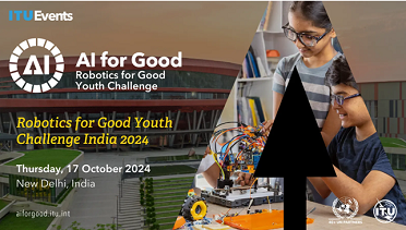
IIT Delhi’s Technology Innovation Hub IHFC, ITU Collaborate to Organise ‘Robotics for Good Youth Challenge’
Read More
2nd online CEP programme on "Executive Programme in Product Innovation and Design Thinking for Business Growth".
Read More
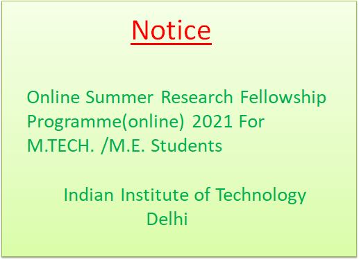
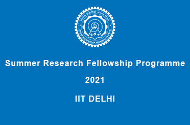
SUMMER RESEARCH FELLOWSHIP PROGRAMME 2024 FOR M.TECH. /M.E. STUDENTS AT INDIAN INSTITUTE OF TECHNOLOGY DELHI
Read More
QS World University Rankings by Subject 2024: IIT Delhi Ranked Among the Top 100 World Institutions in 08 Specific Subject Areas; Features Among Top 50 in Engineering and Technology
Read More
International Women's Day: Talk titled "Rise to Shine: Embracing Challenges for Success” Organised
Read More
Antara Senior Care Signs MoU with IIT Delhi to Design Innovative Mobility-aid Solutions for Seniors
Read More
Israel Aerospace Industries and IIT Delhi Sign CSR Agreement to Collaborate on Applied Research
Read More
IIT Delhi’s Department of Humanities and Social Sciences to Offer a New Academic Program ‘M.A. in Culture, Society, Thought’
Read More
Completion of Sequencing of 10000 Genomes of Indian Population: IIT Delhi Scientists Make Significant Contribution
Read More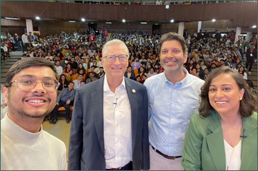
Bill Gates Inspires IIT Delhi Students, Encourages Them to Apply Their Skills to Global Challenges
Read More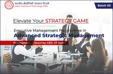
03rd online CEP programme titled "Executive Management Programme in Advanced Strategic Management"
Read More
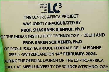
LC3-TRC Africa Project Mentored by IIT Delhi Researchers Inaugurated at Kenya’s Meru University of Science and Technology
Read More
R Systems International Ltd. and IIT Delhi Partner to Set Up a Centre of Excellence on Applied AI for Sustainable Systems
Read More
Transformative Leadership in STEMM (TLS) Workshop for Ph.D. Scholars from SC/ST Community Held at IIT Delhi
Read More
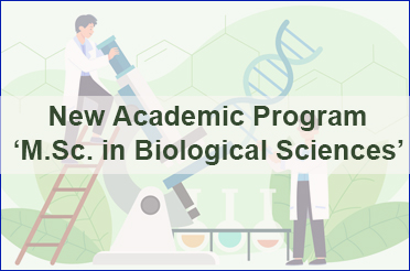
IIT Delhi Launches a New Academic Program ‘M.Sc. in Biological Sciences’; Admissions Through JAM
Read More
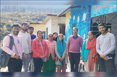
GRIP: IIT Delhi Students Visit Uttarakhand Villages; Will Develop Tech Solutions to Address Issues Faced by Local Population
Read More
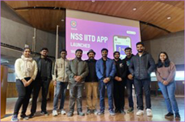
National Service Scheme (NSS) of IIT Delhi Launches an In-house-developed Mobile App, Making Volunteering Much More Accessible
Read More
Call for Applications: Transformative Leadership in STEMM (TLS) Workshop for Advanced PhD Scholars from SC/ST community.
Read More

Request for Proposal: Empanelment of Service providers for the Online CEP Programmes at IIT Delhi
Read More

2nd online CEP programme titled "Executive Programme in Healthcare Entrepreneurship and Management"
Read More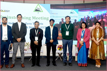
Consultative Brainstorming Meeting: ‘DST's Roadmap Towards India’s Net Zero Targets Through Carbon Capture, Utilization, and Storage’
Read More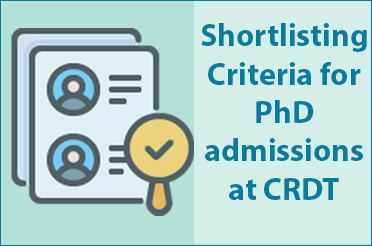
04th online CEP programme titled "Certification in Quantum Computing and Machine Learning"
Read More
IIT Delhi Faculty Combines Technology with Art Forms to Offer a Holistic Educational Experience to Materials Engineering Students
Read More
Placement Season Begins at IIT Delhi- Students Receive 480 Job Offers By the End of December 1
Read More
Over 30 High School Girls Successfully Complete Second STEM Mentorship Program Launched by IIT Delhi
Read More
BioTEX-2023 : Organized by the CBME, Indian Institute of Technology (IIT) Delhi at New Delhi from 27th November-1st December 2023
Read More
Shortlisting Criteria and List of candidates shortlisted for interview for the MSR Program in the Department of Materials Science and Engineering for the session 2023-24, II Semester
Read More
Short-listing criteria for admission to Ph.D. in Materials Science and Engineering for the year 2023-2024 (2nd Semester)
Read More
IIT DELHI ANNOUNCES M. TECH. IN ENERGY TRANSITION AND SUSTAINABILITY FOR THE ABU DHABI CAMPUS: Last date extended to November 30, 2023
Read More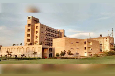
3rd online CEP programme titled "Advanced Certification in Data Science and Decision Science"
Read More
online CEP programme titled "Hands-on Training on "Semiconductor Device Technology: Fabrication and Characterization"
Read More
IIT Delhi Faculty Prof. Shilpi Sharma and Prof. Anurag Singh Rathore Win Tata Transformation Prize; Recognized for their Cutting-Edge Solutions to Food Security and Healthcare
Read More
Hon'ble Vice-President of India, Shri Jagdeep Dhankhar, Visits IIT Delhi and Interacts with Students
Read More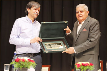
In pictures: Hon'ble Vice-President of India, Shri Jagdeep Dhankhar, Visits IIT Delhi and Interacts with Students
Read More
Tehri Hydro Development Corporation India Limited (THDCIL) and IIT Delhi Ink MoU for Transformative Research and Development Initiatives
Read More
DAKSH Centre of Excellence for Law and Technology at IIT Delhi Launches a Book Titled ‘Technology and Analytics for Law and Justice’
Read More
IIT Delhi and HORIBA India Jointly Hold Tech Symposium on ‘Solutions for Semiconductor Industry’
Read More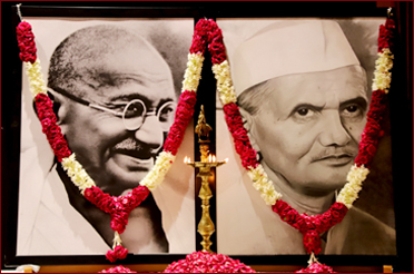
In pictures: Birth Anniversary of Mahatma Gandhi and Shri Lal Bahadur Shastri Celebrated at IIT Delhi
Read More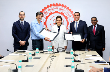

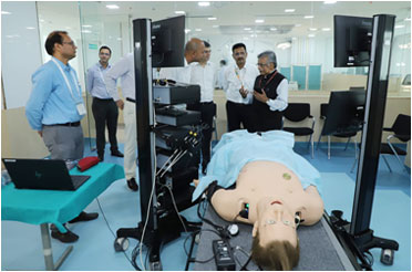
First of Its Kind ‘Medical Cobotics Centre (MCC)’ Inaugurated in New Delhi; to Foster Innovation in Healthcare
Read More
online CEP programme titled "Certificate Programme in Project Management: Theory & Practice"
Read More
IIT Delhi’s Prof. Dipti Ranjan Sahoo Wins Shanti Swarup Bhatnagar Prize for Science and Technology 2022
Read More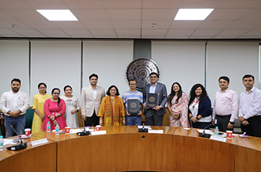
IIT Delhi and EXL Enter into MoU to Work Towards Empowering Women Entrepreneurs Through Digital and Financial Literacy
Read More
2nd online CEP programme titled "Executive Management Programme in Advanced Strategic Management"
Read More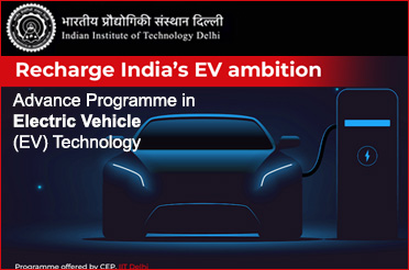
First Batch of UQIDAR Students Receive Joint PhD Degree at 54th IIT Delhi Convocation Ceremony
Read More
In pictures: IIT Delhi Celebrates Independence Day; Employees Awarded for Exemplary Contribution to Institute
Read More
IIT Delhi's School of Public Policy Successfully Places its Inaugural Masters in Public Policy Batch
Read More
Workshop on MedTech and Healthcare Ecosystem for Upcoming IIT Delhi - Jhajjar Campus Organised
Read More
2357 Graduating IIT Delhi Students Receive Degrees and Diplomas at the 54th Annual Convocation Ceremony
Read More
IIT Delhi to Hold its 54th Convocation on August 12; Eminent Virologist Dr. Gagandeep Kang to be the Chief Guest
Read More
_1691059736.jpg)

IIT Delhi Successfully Organizes Open House for JEE (Advanced) 2023 Qualified Female and PwD Candidates
Read More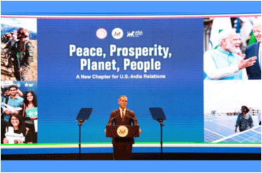
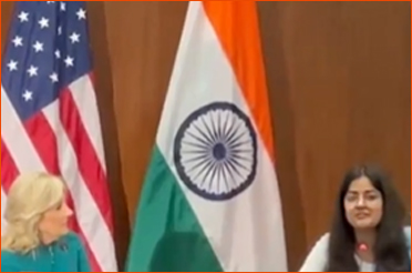
IIT Delhi Research Scholar Anchal Sharma Makes Research Presentation Before Indian PM and US First Lady at NSF
Read More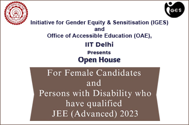
IIT Delhi is organising an Open House for JEE (Advanced) 2023 qualified Female and Pwd Candidates on June 24, 2023 (Saturday)
Read More
online CEP programme titled "Applied Data Science using Machine Learning & Artificial Intelligence"
Read More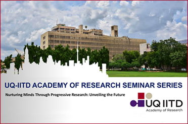
IIT Delhi Celebrates World Telecommunication Day; India’s G20 Sherpa, Mr. Amitabh Kant, Delivers Annual Bharti Lecture
Read More
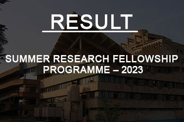

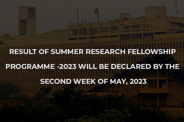
RESULT OF SUMMER RESEARCH FELLOWSHIP PROGRAMME -2023 WILL BE DECLARED BY THE SECOND WEEK OF MAY, 2023
Read More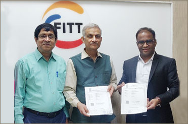
MechAnalyzer Software to Help Engineering Students Learn Concepts of Mechanisms; FITT-IIT Delhi and SVR InfoTech Sign MoU for Sale and Tech Support
Read More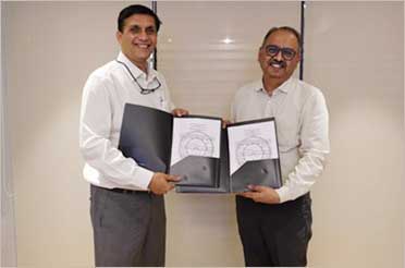
Venus Chair Established at IIT Delhi to Support Teaching and Research & Development in the Area of Fibrous Air Filters
Read More
Deadline of Submission of Online Applications for SRFP - 2023 extended upto 19.04.2023 till 11:59 PM
Read More
2nd online CEP programme titled "Advanced Certification in Data Science and Decision Science (Batch 2) "
Read More
IIT Delhi’s Two-Day Annual Career Fest ‘Pravritti 2023- Expanding Horizons’ to Begin on April
Read More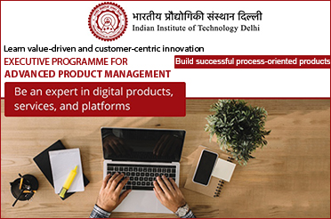
2nd online CEP programme titled "Executive Programme for Advanced Product Management (Batch 2)"
Read More
online CEP programme titled "Executive Programme in Product Innovation & Design Thinking for Business Growth"
Read More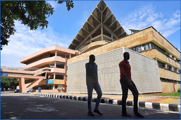
QS World University Rankings by Subject 2023: IIT Delhi Among the Top 50 Institutions in the World in Engineering & Technology with 48th Rank
Read More
MoS for Education Dr. Subhas Sarkar Inaugurates Unnat Bharat Abhiyan's "UNNATI Mahotsav and Expo" at IIT Delhi
Read More
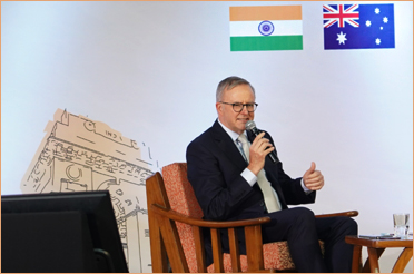
In pictures- Hon'ble Australian PM Mr. Anthony Albanese's Visit to IIT Delhi on March 10, 2023
Read More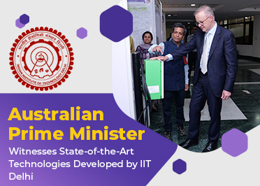
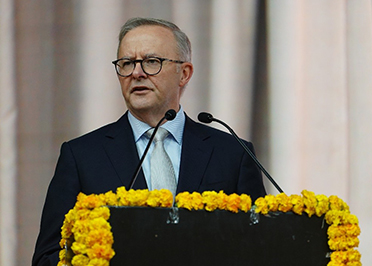
Hon’ble Australian Prime Minister Mr. Anthony Albanese Visits IIT Delhi; Addresses Students
Read More
IIT Delhi’s Three-day Annual Science, Technology and Management Festival “Tryst 2023” Kicks Off
Read More
IIT Delhi Alumnus Alok Aggarwal Endows Chair for Research in ESG (Environmental, Social, and Governance) Area
Read More
IIT Delhi to Develop Smart Monitoring System to Ensure Safety of Persons Working at Height
Read More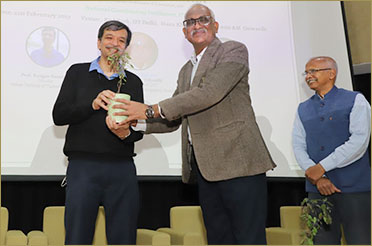
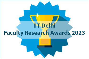
65th Foundation Day of IIT Delhi Celebrated; Faculty Research Awards 2022 Presented on Foundation Day
Read More
Mobility for All: Continental with IIT Delhi Develop A Solution for Visually Impaired To Access Public Buses
Read More
27th Inter-IIT Staff Sports Meet: IIT Delhi Wins Overall Championship and General Championship (Men)
Read More
IIT Delhi Placement Drive 2022-23: Students Receive Record Number of Job Offers Up to December 15
Read More
IIT Delhi and University of Helsinki, Finland, Sign MoU for Academic Cooperation; Aims to Contribute to Solving Air Quality and Climate Change Challenges in India
Read More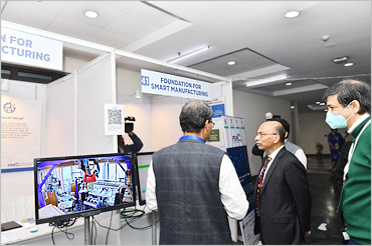
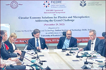
CRDT, IIT Delhi Organises International Symposium on Circular Economy Solutions for Plastics and Microplastics jointly with University of Eastern Finland (UEF)
Read More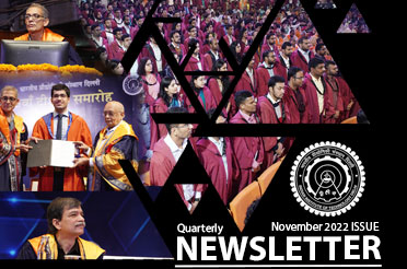
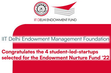
Four Startups led by IIT Delhi Students Win a Grant of Rs 50 lakh Each Under Endowment Nurture Fund Initiative
Read More
Advertisement inviting applications for the post of Director, IIT IIT Kanpur and IIT (ISM) Dhanbad
Read More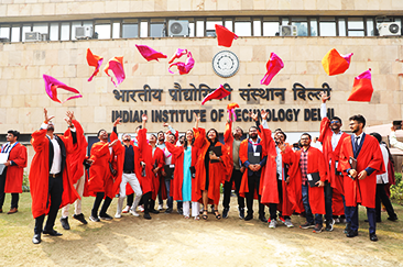
IIT Delhi Holds 53rd Annual Convocation Ceremony; 2100 Graduating Students Awarded Degrees and Diplomas
Read More
Rural Technology Action Group (RuTAG) at IIT Delhi Transfers Two Technologies to Four African Nations
Read More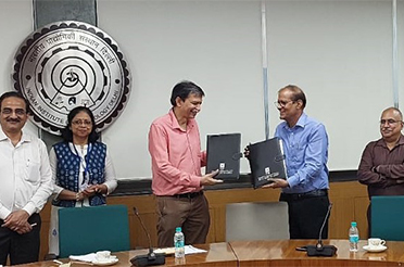
Department of Telecommunications R&D Centre C-DOT and IIT Delhi Sign MoU for Cooperation in Various Emerging Areas of Telecom
Read More
Workshop on Addressing Air Quality Challenges in Delhi-NCT Held at IIT Delhi; Team Sweden, IIT Delhi Identify Possible Areas of Joint Intervention
Read More
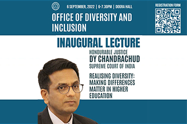
Supreme Court Judge Hon’ble Justice D.Y. Chandrachud to Deliver Inaugural Talk for the Office of Diversity and Inclusion at IIT Delhi
Read More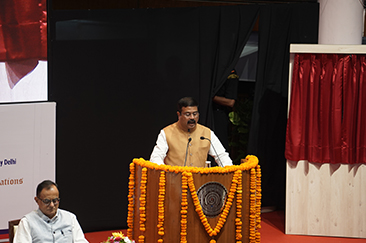
Hon’ble Union Education Minister, Shri Dharmendra Pradhan Addresses IIT Delhi Diamond Jubilee Celebrations Closing Ceremony
Read More
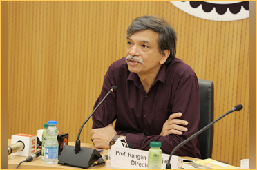
IIT Delhi Diamond Jubilee Celebrations Closing Ceremony- Director Prof. Rangan Banerjee's Speech
Read More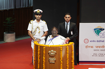
IIT Delhi Diamond Jubilee Celebrations Closing Ceremony- Hon'ble President of India, Smt. Droupadi Murmu's Speech
Read More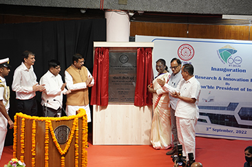
Hon’ble President of India, Smt. Droupadi Murmu Graces IIT Delhi Diamond Jubilee Celebrations Closing Ceremony
Read More
FSAE Italy 2022- IIT Delhi’s Automobile Club AXLR8R Formula Racing Secures First Position in Cost and Manufacturing Event
Read More
Union Minister Shri Piyush Goyal Inaugurates Public Systems Lab at IIT Delhi Established in Partnership with UNWFP
Read More
IIT Delhi’s Technology Innovation Hub IHFC Gets 12 Projects Under DST-NSF Joint Research and Development Program
Read More
_1659327288.jpg)
IIT Delhi Organises Academic Outreach Day for Students and Faculty of Haryana Govt. Technical Universities and Colleges
Read More
NIRF India Rankings 2022- IIT Delhi Achieves 2nd Rank in Engineering; Jumps to 4th in Management; Features Among Top 3 Research Institutes
Read More
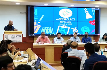
mPRAGATI, a One Stop MedTech Technology Development Facility at IIT Delhi Under ICMR-Medical Device and Diagnostics Mission Secretariat, Unveiled
Read More
Empanelment of retired officers as an Inquiry Officers for conducting Departmental Inquiry - reg.
Read More
First Batch Successfully Completes IIT Delhi’s STEM Mentorship Program for High Schoolgirls
Read More
School students showcase promising prototypes they built at Change.Makers summer boot camp organised by IIT Delhi
Read More
IITs in Delhi, Bombay and Kanpur Offer Internship and Sponsored M. Tech. Programmes to Students from Ladakh
Read More
IHFC, TIH of IIT Delhi, Celebrates its 2nd Anniversary; Announces Call for Proposal in Areas of Autonomous Vehicles, Nano Robotics, Block Chain for Applications in Robotics
Read More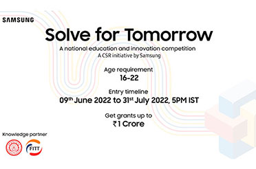
Samsung Launches ‘Solve for Tomorrow’, an Innovation Contest for India’s Youth to Crack Real-World Problems; FITT at IIT Delhi to be the Knowledge Partner
Read More
QS World University Rankings 2023- IIT Delhi Achieves an Improved Overall Rank of 174 Globally
Read More

DEPARTMENT OF HUMANITIES AND SOCIAL SCIENCES, IIT DELHI --- Indian & Foreign Languages Learning Programme
Read More
Result- UG - Summer Research Fellowship Programme - 2022 ( IN CONTINUATION TO THE LIST OF STUDENTS PUBLISHED on 13th May, 2022 )
Read More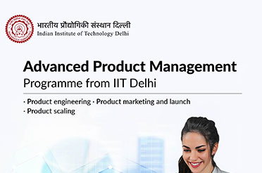
Technology Innovation Hub of IIT Delhi (IHFC) Signs MoU with the Council for the Indian School Certificate Examinations (CISCE)
Read More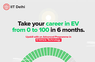

_1651059243.png)

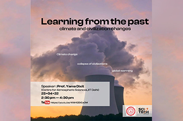
Did Climate Change Cause Ancient Civilizations to Collapse? 08thIIT Delhi SciTech Spins Lecture to Explain
Read More
PG Admission including Ph.D. - Last date for submission of online application and application fee has been extended to April 17, 2022 (4 pm). No further extension will be made.
Read More
QS World University Rankings by Subject 2022 - Five IIT Delhi Academic Programmes in Top 100
Read More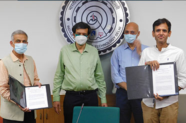
IIT Delhi, Delhi Jal Board Sign MoU to Address Water Security Issues Faced by NCT of Delhi
Read More
World Class Indoor Sports Complex Built with Alumnus Saurabh Mittal's Support Inaugurated at IIT Delhi
Read More
2nd online CEP Certificate programme titled Executive Management Programme in Entrepreneurship Development (EMPED)
Read More
Fabiosys Innovations, an IIT Delhi Startup, Develops Technology to Manufacture Extremely Affordable and Highly Effective Antiviral Fabric
Read More
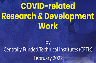
COVID-related Research & Development Work by Centrally Funded Technical Institutes (CFTIs), Ministry of Education, Government of India - February 2022
Read More
IHFC, Technology Innovation Hub of IIT Delhi, Collaborates with US’ National Science Foundation for Research in Cobotics, AI
Read More
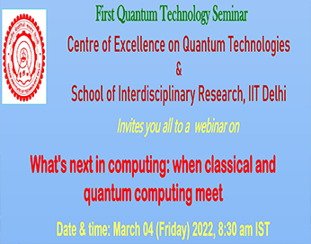
Webinar on "What's next in computing: when classical and quantum computing meet" by Dr. Mukesh V. Khare, Vice President, Semiconductor & Cloud, IBM Research, USA on March 04 (Friday) 2022, 8:30 AM IST
Read More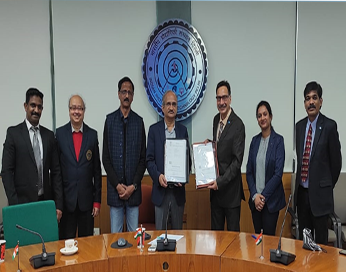
HORIBA India, IIT Delhi Join Hands to Establish Research Center at the Institute’s Chemistry Department
Read More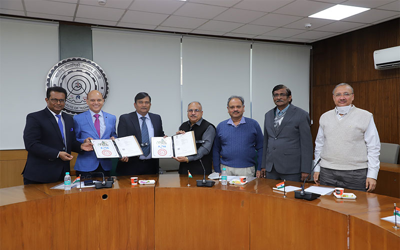
Troop Comforts Ltd Signs MoU with IIT Delhi to Develop Smart Protective Clothing for Indian Security Forces
Read More
SciTech Spins Lecture: School Students to Learn About Role of Imaging in Advancing Science and Technology
Read More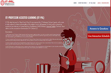
IIT Delhi Launches an Interactive Website of IIT-PAL to Help High School Students Prepare for Competitive Exams
Read More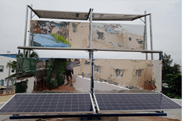
IIT Delhi Researchers Develop High Efficiency, Shadow-less, Portable Solar PV Towers for Power Generation
Read More

IIT Delhi Sets up “Pillay Chair Professor” for Research in Machine Learning, VLSI Design and Sensors
Read More
IIT Delhi Students Receive Record Number of Job Offers Up to December 15 of Placement Drive 2021
Read More
SciTech Spins 4th Lecture: School Students to Learn About Mysteries of Universe from IIT Delhi Scientists
Read More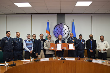
IIT Delhi’s State of the Art Research & Innovation Park Wins Prestigious Façade Project of the Year Award 2021
Read More
Brain Storming Conclave on Atmanirbhar North East through S&T Interventions at Cotton University, Guwahati, Assam December 21–22, 2021
Read More
IntelliSmart & IIT Delhi collaborate to develop next generation Smart Grid technology solutions & capabilities
Read More
IIT Delhi Collaborates with National Law University Delhi for Ushering in Tech-empowered Justice System
Read More
IIT Delhi and Business Sweden - The Swedish Trade and Invest Council Sign MoU for Clean Air and Green Energy Collaborations
Read More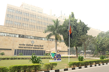
Neilom Prize 2020-21: Recent Graduates of IIT Delhi Awarded for their Work in the Field of Assistive Technology
Read More
‘Why did the Titanic Sink?’ 3rd SciTech Spins Lecture by IIT Delhi to Explain This and Many More Questions to School Students
Read More
Technology Innovation Hubs of IIT Delhi and IIIT Delhi Sign MoU to set up India’s First Medical Cobotics Centre
Read More
State-of-the-art Laboratories Inaugurated at IIT Delhi’s Centre Focusing on Electric Vehicle Technologies
Read More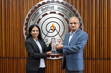

IIT Delhi, AIIMS New Delhi Jointly Establish Centre for Advanced Research and Excellence in Disability & Assistive Technology (CARE-DAT), a Centre of Excellence
Read More
IIT Delhi’s School of Artificial Intelligence to Start ‘M.Tech in Machine Intelligence & Data Science (MINDS)’
Read More
Applications are invited for appointment to the post of Director, Indian Institute of Technology (llT) Bhubaneswar
Read More
Advertisement inviting applications for the post of Director, IIT Palakkad, IIT Tirupati, IIT Dharwad, IIT Bhilai, IIT Goa and IIT Jammu
Read More
IIT Delhi to Teach School Students ‘How Powerful Computers Can Help in Providing Insights into Real-Life Phenomena’
Read More
IIT Delhi Announces Scholarships and Seed Funding Programs to Mark 2nd Anniversary of its Alumni Endowment Fund
Read More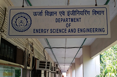
IIT Delhi Launches New UG Programme ‘B. Tech. in Energy Engineering’; JEE (Advanced) Qualified Students Eligible
Read More
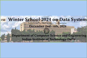
Alumnus Mohit Aron Gifts USD 1 Million to IIT Delhi’s Computer Science and Engineering Department
Read More

B.Tech. Students of NIT Sikkim to be Eligible for Direct Admission to IIT Delhi’s PhD Programmes
Read More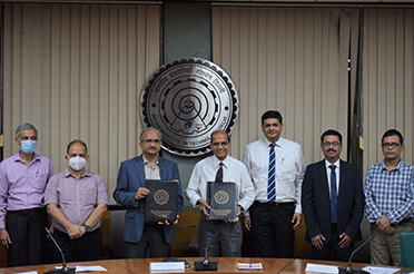
JK Paper Signs MoU with IIT Delhi to Set Up JK Paper Centre of Excellence in Paper and Packaging
Read More
IIT Delhi’s Over Rs 500 Cr State-of-the Art ‘Central Research Facility’ Now Open for Researchers from Across Country
Read More

Optics and Photonics Centre of IIT Delhi launches an outreach initiative named "Optics Learning Centre"
Read More

IIT Delhi Launches Sci-Tech Spins - A Series of Weekend Seminars & Laboratory Demos for High School Students
Read More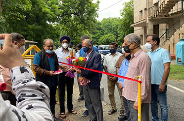
DAKSH Centre of Excellence (CoE) for Law & Technology, IIT Delhi Releases Report on Six High Court Websites
Read More
"ComIN21 Asian Voices in Pandemic" conference organized by the Department of Design, IIT Delhi in December 2021
Read More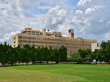
Seminar on Benefits and Challenges in the Next Decade of Semiconductor Innovation by Dr. Randhir Thakur, Senior Vice President, Intel, USA on 19.08.2021 at 10:00 am
Read More
Unnat Bharat Abhiyan Announces Results of Regional Level Poster and Video Competition for COVID-19 Awareness
Read More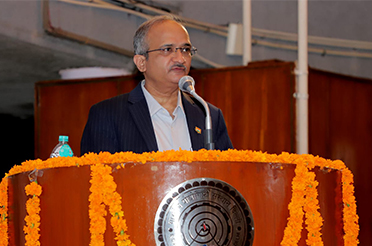
Vipula and Mahesh Chaturvedi Foundation Signs MoU to Attract Outstanding Talent to IIT Delhi
Read More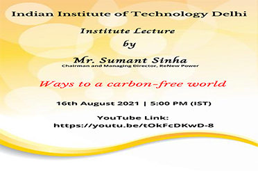
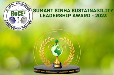
An Institute Lecture on "Ways to a Carbon-free world" by Mr. Sumant Sinha, Chairman and Managing Director, ReNew Power
Read More
National Health Authority and Indian Institute of Technology Delhi join hands to scale high-potential healthcare innovations
Read More
Attention 2020 Entry UG students: Final list of UG students (2020 Entry) for Change of Programme at the end of 1st Year
Read More
IIT Delhi Establishes Chairs to Support Research in Microelectronics & VLSI Design and Geotechnical & Geo-Environmental Engineering
Read More
IFFCO Signs MoU with IIT Delhi for Innovative & Collaborative Projects to Bring Labs to Farms
Read More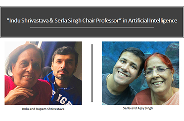
IIT Delhi Alumni Endow Indu Shrivastava & Serla Singh Chair Professor in Artificial Intelligence
Read More
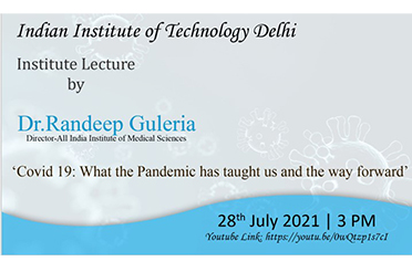
Covid-19: What the pandemic has taught us and the way forward lecture by Prof./Dr. Randeep Guleria, Director, All India Institute of Medical Science (AIIMS), Delhi
Read More
IIT Delhi Establishes Manish Singhal Chair to Promote Teaching and Research in the Area of Smart Textiles
Read More
Supreme Court Judge Mr. Justice S. Ravindra Bhat inaugurates UJF Lab Facility on AI for Judiciary at IIT Delhi
Read More

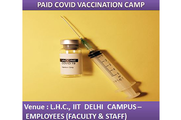
PAID COVID VACCINATION CAMP - COVISHIELD - 8TH JUNE, 2021 (Tuesday), L.H.C., IIT CAMPUS - EMPLOYEES (FACULTY & STAFF)
Read More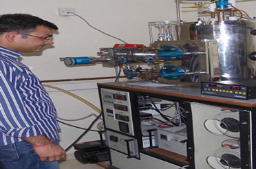
IIT Delhi to Establish Department of Energy Science and Engineering: New UG Programme B.Tech. in Energy Engineering To Be Offered from This Year
Read More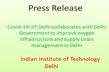
Covid-19: IIT Delhi collaborates with Delhi Government to improve oxygen infrastructure and supply chain management in Delhi
Read More
IIT Delhi to Create New Centre to Synergize and Boost R&D Activities in Optics and Photonics Field
Read More
Short-listing criteria for admission to Ph.D. in Materials Science and Engineering for the year 2021-2022 (I Semester) and List of Shortlisted candidates for PhD Interview
Read More
Short-listing criteria for admission to MS(R) in Materials Science and Engineering for 2021-22 (I Semester) & List of Shortlisted candidates for MS (R) Interview
Read More